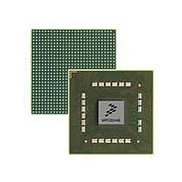
MPC8544VTALF Freescale Semiconductor, MPC8544VTALF Datasheet - Page 717

MPC8544VTALF
Manufacturer Part Number
MPC8544VTALF
Description
MPU POWERQUICC III 783-PBGA
Manufacturer
Freescale Semiconductor
Datasheets
1.MPC8544VTALF.pdf
(117 pages)
2.MPC8544VTALF.pdf
(2 pages)
3.MPC8544VTALF.pdf
(1340 pages)
Specifications of MPC8544VTALF
Processor Type
MPC85xx PowerQUICC III 32-Bit
Speed
667MHz
Voltage
1V
Mounting Type
Surface Mount
Package / Case
783-FCPBGA
Processor Series
MPC85xx
Core
e500
Data Bus Width
32 bit
Maximum Clock Frequency
667 MHz
Maximum Operating Temperature
+ 105 C
Mounting Style
SMD/SMT
Data Ram Size
32 KB
I/o Voltage
1.8 V, 3.3 V
Interface Type
I2C, HSSI, DUART
Minimum Operating Temperature
0 C
Lead Free Status / RoHS Status
Lead free / RoHS Compliant
Features
-
Lead Free Status / Rohs Status
Lead free / RoHS Compliant
Available stocks
Company
Part Number
Manufacturer
Quantity
Price
Company:
Part Number:
MPC8544VTALF
Manufacturer:
Freescale Semiconductor
Quantity:
10 000
Company:
Part Number:
MPC8544VTALFA
Manufacturer:
Freescale Semiconductor
Quantity:
10 000
- Current page: 717 of 1340
- Download datasheet (12Mb)
ZBT SRAMs perform four-beat bursts. Because the LBC generates eight-beat transactions (for 32-bit
ports) the UPM breaks down each burst into two consecutive four-beat bursts. The internal address
generator of the LBC generates the new A27 for the second burst.
Because we use linear burst on the SRAM, the device will itself burst with the burst addresses of [0:1:2:3].
The local bus always generates linear bursts and expects [0:1:2:3:4:5:6:7]. Therefore, two consecutive
linear bursts of the ZBT SRAM with A27 = 0 for the first burst and A27 = 1 for the second burst give the
desired burst pattern.
The UPM also supports single beat accesses. Because the ZBT SRAM does not support this and always
responds with a burst, the UPM pattern has to take care that data for the critical beat is provided (for write)
or sampled (for read), and that the rest of the burst is ignored (by negating WE). The UPM controller
basically has to wait for the end of the SRAM burst to avoid bus contention with further bus activities.
ZBT SRAMs have a power down mode, which is invoked by the ZZ signal. Connecting a GPIO signal to
ZZ allows use of that power down mode; however, accesses to the SRAM while in power down mode do
not create valid results. This should be taken care of by the system software.
Another observation is that SRAMs are available with natural parity. In the example, we use a ×18 SRAM,
which holds two data bytes and two parity bits. While for the support of parity on SDRAM banks the local
Freescale Semiconductor
Local Bus Interface
MPC8544E PowerQUICC III Integrated Host Processor Family Reference Manual, Rev. 1
LAD[0:31]
LA[27:29]
LBS[0:3]
LDP[0:3]
LGPL0
LGPL1
LGPL2
LCS n
GPIO
LALE
LCLK
Latch
Figure 14-79. Interface to ZBT SRAM
BW[0:1]
DATA[0:15]
OE
CE
ADV/LD
WE
ZZ
BW[0:1]
MODE
CKE
CLK
SA[19:0]
DQ[0:17]
1M × 18
SRAM
ZBT
DP[0:1]
BW[2:3]
DATA[16:31]
OE
CE
ADV/LD
WE
ZZ
BW[0:1]
MODE
CKE
CLK
SA[19:0]
DQ[0:17]
1M × 18
SRAM
ZBT
Local Bus Controller
DP[2:3]
14-97
Related parts for MPC8544VTALF
Image
Part Number
Description
Manufacturer
Datasheet
Request
R
Part Number:
Description:
Manufacturer:
Freescale Semiconductor, Inc
Datasheet:
Part Number:
Description:
Manufacturer:
Freescale Semiconductor, Inc
Datasheet:
Part Number:
Description:
Manufacturer:
Freescale Semiconductor, Inc
Datasheet:
Part Number:
Description:
Manufacturer:
Freescale Semiconductor, Inc
Datasheet:
Part Number:
Description:
Manufacturer:
Freescale Semiconductor, Inc
Datasheet:
Part Number:
Description:
Manufacturer:
Freescale Semiconductor, Inc
Datasheet:
Part Number:
Description:
Manufacturer:
Freescale Semiconductor, Inc
Datasheet:
Part Number:
Description:
Manufacturer:
Freescale Semiconductor, Inc
Datasheet:
Part Number:
Description:
Manufacturer:
Freescale Semiconductor, Inc
Datasheet:
Part Number:
Description:
Manufacturer:
Freescale Semiconductor, Inc
Datasheet:
Part Number:
Description:
Manufacturer:
Freescale Semiconductor, Inc
Datasheet:
Part Number:
Description:
Manufacturer:
Freescale Semiconductor, Inc
Datasheet:
Part Number:
Description:
Manufacturer:
Freescale Semiconductor, Inc
Datasheet:
Part Number:
Description:
Manufacturer:
Freescale Semiconductor, Inc
Datasheet:
Part Number:
Description:
Manufacturer:
Freescale Semiconductor, Inc
Datasheet:


