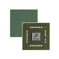
MPC8544VTALF Freescale Semiconductor, MPC8544VTALF Datasheet - Page 633

MPC8544VTALF
Manufacturer Part Number
MPC8544VTALF
Description
MPU POWERQUICC III 783-PBGA
Manufacturer
Freescale Semiconductor
Datasheets
1.MPC8544VTALF.pdf
(117 pages)
2.MPC8544VTALF.pdf
(2 pages)
3.MPC8544VTALF.pdf
(1340 pages)
Specifications of MPC8544VTALF
Processor Type
MPC85xx PowerQUICC III 32-Bit
Speed
667MHz
Voltage
1V
Mounting Type
Surface Mount
Package / Case
783-FCPBGA
Processor Series
MPC85xx
Core
e500
Data Bus Width
32 bit
Maximum Clock Frequency
667 MHz
Maximum Operating Temperature
+ 105 C
Mounting Style
SMD/SMT
Data Ram Size
32 KB
I/o Voltage
1.8 V, 3.3 V
Interface Type
I2C, HSSI, DUART
Minimum Operating Temperature
0 C
Lead Free Status / RoHS Status
Lead free / RoHS Compliant
Features
-
Lead Free Status / Rohs Status
Lead free / RoHS Compliant
Available stocks
Company
Part Number
Manufacturer
Quantity
Price
Company:
Part Number:
MPC8544VTALF
Manufacturer:
Freescale Semiconductor
Quantity:
10 000
Company:
Part Number:
MPC8544VTALFA
Manufacturer:
Freescale Semiconductor
Quantity:
10 000
- Current page: 633 of 1340
- Download datasheet (12Mb)
1
14.3.1.2.2
Figure 14-3
Reset OR1–7
Table 14-6
Freescale Semiconductor
17–18
21–22
OR0 has this value set during reset (GPCM is the default control machine for all banks coming out of reset). All other option
registers have all bits cleared.
0–16
Bits
Reset OR0 0 0 0 0 0 0 0 0 0 0 0 0 0 0 0 0 0 0 0
19
20
Offset 0x004 (OR0)
BCTLD Buffer control disable. Disables assertion of LBCTL during access to the current memory bank.
Name
CSNT Chip select negation time. Determines when LCS n and LWE are negated during an external memory write
XAM
ACS
W
AM
R
describes ORn fields for GPCM mode.
shows the bit fields for ORn when the corresponding BRn[MSEL] selects the GPCM machine.
0x00C (OR1)
0x014 (OR2)
0x01C (OR3)
0
MPC8544E PowerQUICC III Integrated Host Processor Family Reference Manual, Rev. 1
GPCM address mask. Masks corresponding BR n bits. Masking address bits independently allows external
devices of different size address ranges to be used. Address mask bits can be set or cleared in any order in
the field, allowing a resource to reside in more than one area of the address map.
0 Corresponding address bits are masked.
1 Corresponding address bits are used in the comparison between base and transaction addresses.
Extended address mask. Masks the corresponding XBA bits in the BR n register, effectively extending the
address mask (AM) by 2 bits.
0 LBCTL is asserted upon access to the current memory bank.
1 LBCTL is not asserted upon access to the current memory bank.
access handled by the GPCM, provided that ACS ≠ 00 (when ACS = 00, only LWE is affected by the setting
of CSNT). This helps meet address/data hold times for slow memories and peripherals.
0 LCS n and LWE are negated normally.
1 LCS n and LWE are negated one quarter of a bus clock cycle earlier.
Address to chip-select setup. Determines the delay of the LCS n assertion relative to the address change
when the external memory access is handled by the GPCM. At system reset, OR0[ACS] = 11.
Option Registers (OR n )—GPCM Mode
Value
00
01
10
11
AM
Figure 14-3. Option Registers (OR n ) in GPCM Mode
Table 14-6. OR n
0x024 (OR4)
0x02C (OR5)
0x034 (OR6)
0x03C (OR7)
LCS n is output at the same time as the address lines. Note that this overrides the
value of CSNT such that CSNT=0.
Reserved.
LCS n is output a quarter bus clock cycle after the address lines.
LCS n is output a half bus clock cycle after the address lines.
16 17 18
XAM BCTLD CSNT ACS XACS
—
GPCM Field Descriptions
19
0
Description
All zeros
20
1
21 22
1 1
Meaning
23
1
24
1 1 1 1
SCY
27
SETA TRLX EHTR EAD
28
0
Access: Read/Write
Local Bus Controller
29
1
30
1
14-13
31
1
1
Related parts for MPC8544VTALF
Image
Part Number
Description
Manufacturer
Datasheet
Request
R
Part Number:
Description:
Manufacturer:
Freescale Semiconductor, Inc
Datasheet:
Part Number:
Description:
Manufacturer:
Freescale Semiconductor, Inc
Datasheet:
Part Number:
Description:
Manufacturer:
Freescale Semiconductor, Inc
Datasheet:
Part Number:
Description:
Manufacturer:
Freescale Semiconductor, Inc
Datasheet:
Part Number:
Description:
Manufacturer:
Freescale Semiconductor, Inc
Datasheet:
Part Number:
Description:
Manufacturer:
Freescale Semiconductor, Inc
Datasheet:
Part Number:
Description:
Manufacturer:
Freescale Semiconductor, Inc
Datasheet:
Part Number:
Description:
Manufacturer:
Freescale Semiconductor, Inc
Datasheet:
Part Number:
Description:
Manufacturer:
Freescale Semiconductor, Inc
Datasheet:
Part Number:
Description:
Manufacturer:
Freescale Semiconductor, Inc
Datasheet:
Part Number:
Description:
Manufacturer:
Freescale Semiconductor, Inc
Datasheet:
Part Number:
Description:
Manufacturer:
Freescale Semiconductor, Inc
Datasheet:
Part Number:
Description:
Manufacturer:
Freescale Semiconductor, Inc
Datasheet:
Part Number:
Description:
Manufacturer:
Freescale Semiconductor, Inc
Datasheet:
Part Number:
Description:
Manufacturer:
Freescale Semiconductor, Inc
Datasheet:


