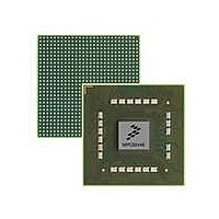
MPC8544VTALF Freescale Semiconductor, MPC8544VTALF Datasheet - Page 681

MPC8544VTALF
Manufacturer Part Number
MPC8544VTALF
Description
MPU POWERQUICC III 783-PBGA
Manufacturer
Freescale Semiconductor
Datasheets
1.MPC8544VTALF.pdf
(117 pages)
2.MPC8544VTALF.pdf
(2 pages)
3.MPC8544VTALF.pdf
(1340 pages)
Specifications of MPC8544VTALF
Processor Type
MPC85xx PowerQUICC III 32-Bit
Speed
667MHz
Voltage
1V
Mounting Type
Surface Mount
Package / Case
783-FCPBGA
Processor Series
MPC85xx
Core
e500
Data Bus Width
32 bit
Maximum Clock Frequency
667 MHz
Maximum Operating Temperature
+ 105 C
Mounting Style
SMD/SMT
Data Ram Size
32 KB
I/o Voltage
1.8 V, 3.3 V
Interface Type
I2C, HSSI, DUART
Minimum Operating Temperature
0 C
Lead Free Status / RoHS Status
Lead free / RoHS Compliant
Features
-
Lead Free Status / Rohs Status
Lead free / RoHS Compliant
Available stocks
Company
Part Number
Manufacturer
Quantity
Price
Company:
Part Number:
MPC8544VTALF
Manufacturer:
Freescale Semiconductor
Quantity:
10 000
Company:
Part Number:
MPC8544VTALFA
Manufacturer:
Freescale Semiconductor
Quantity:
10 000
- Current page: 681 of 1340
- Download datasheet (12Mb)
The user must ensure that patterns for single-beat transfers contain one, and only one, transfer
acknowledge (UTA bit in RAM word set high) and for a burst transfer, contain the exact number of transfer
acknowledges required.
Any transfers that do not naturally fit single or burst transfers are synthesized as a series of single transfers.
These accesses are treated by the UPM as back-to-back, single-beat transfers. Burst transfers can also be
inhibited by setting ORn[BI]. Burst performance can be achieved by ensuring that UPM transactions are
32-byte aligned with a transaction size being some multiple of 32-bytes, which is a natural fit for
cache-line transfers, for example.
14.4.4.1.2
Each UPM contains a refresh timer that can be programmed to generate refresh service requests of a
particular pattern in the RAM array.
memory refresh timer request generation. The UPM refresh timer register (LURT) defines the period for
the timers associated with all three UPMs.
By default, all local bus refreshes are performed using the refresh pattern of UPMA. This means that if
refresh is required, MAMR[RFEN] must be set. It also means that only one refresh routine should be
programmed and be placed in UPMA, which serves as the refresh executor. Any banks assigned to a UPM
are provided with the refresh pattern if the RFEN bit of the corresponding UPM is set. UPMA assigned
banks, therefore, always receive refresh services when MAMR[RFEN] is set, while UPMB and UPMC
assigned banks also receive (the same) refresh services if the corresponding MxMR[RFEN] bits are set.
Note that the UPM refresh timer request should not be used in a system with SDRAM refresh enabled. The
system designer must choose to use either SDRAM refresh or UPM refresh. Using both may result in
missing refresh periods to memory.
14.4.4.1.3
Software can start a request to the UPM by issuing a RUN command to the UPM. Some memory devices
have their own signal handshaking protocol to put them into special modes, such as self-refresh mode.
Other memory devices require special commands to be issued on their control signals, such as for SDRAM
initialization.
For these special cycles, the user creates a special RAM pattern that can be stored in any unused areas in
the UPM RAM. Then a RUN command is used to run the cycle. The UPM runs the pattern beginning at
the specified RAM location until it encounters a RAM word with its LAST bit set. The RUN command is
issued by setting MxMR[OP] = 11 and accessing UPMn memory region with any write transaction that
hits the corresponding UPM machine. MxMR[MAD] determines the starting address in the RAM array for
the pattern.
Freescale Semiconductor
System Clock
MPC8544E PowerQUICC III Integrated Host Processor Family Reference Manual, Rev. 1
UPM Refresh Timer Requests
Software Requests—RUN Command
Figure 14-55. Memory Refresh Timer Request Block Diagram
PTP Prescaling
Figure 14-55
shows the clock division hardware associated with
Divide by LURT
UPM Refresh Timer Request
Local Bus Controller
14-61
Related parts for MPC8544VTALF
Image
Part Number
Description
Manufacturer
Datasheet
Request
R
Part Number:
Description:
Manufacturer:
Freescale Semiconductor, Inc
Datasheet:
Part Number:
Description:
Manufacturer:
Freescale Semiconductor, Inc
Datasheet:
Part Number:
Description:
Manufacturer:
Freescale Semiconductor, Inc
Datasheet:
Part Number:
Description:
Manufacturer:
Freescale Semiconductor, Inc
Datasheet:
Part Number:
Description:
Manufacturer:
Freescale Semiconductor, Inc
Datasheet:
Part Number:
Description:
Manufacturer:
Freescale Semiconductor, Inc
Datasheet:
Part Number:
Description:
Manufacturer:
Freescale Semiconductor, Inc
Datasheet:
Part Number:
Description:
Manufacturer:
Freescale Semiconductor, Inc
Datasheet:
Part Number:
Description:
Manufacturer:
Freescale Semiconductor, Inc
Datasheet:
Part Number:
Description:
Manufacturer:
Freescale Semiconductor, Inc
Datasheet:
Part Number:
Description:
Manufacturer:
Freescale Semiconductor, Inc
Datasheet:
Part Number:
Description:
Manufacturer:
Freescale Semiconductor, Inc
Datasheet:
Part Number:
Description:
Manufacturer:
Freescale Semiconductor, Inc
Datasheet:
Part Number:
Description:
Manufacturer:
Freescale Semiconductor, Inc
Datasheet:
Part Number:
Description:
Manufacturer:
Freescale Semiconductor, Inc
Datasheet:


