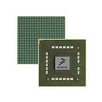
MPC8544VTALF Freescale Semiconductor, MPC8544VTALF Datasheet - Page 542

MPC8544VTALF
Manufacturer Part Number
MPC8544VTALF
Description
MPU POWERQUICC III 783-PBGA
Manufacturer
Freescale Semiconductor
Datasheets
1.MPC8544VTALF.pdf
(117 pages)
2.MPC8544VTALF.pdf
(2 pages)
3.MPC8544VTALF.pdf
(1340 pages)
Specifications of MPC8544VTALF
Processor Type
MPC85xx PowerQUICC III 32-Bit
Speed
667MHz
Voltage
1V
Mounting Type
Surface Mount
Package / Case
783-FCPBGA
Processor Series
MPC85xx
Core
e500
Data Bus Width
32 bit
Maximum Clock Frequency
667 MHz
Maximum Operating Temperature
+ 105 C
Mounting Style
SMD/SMT
Data Ram Size
32 KB
I/o Voltage
1.8 V, 3.3 V
Interface Type
I2C, HSSI, DUART
Minimum Operating Temperature
0 C
Lead Free Status / RoHS Status
Lead free / RoHS Compliant
Features
-
Lead Free Status / Rohs Status
Lead free / RoHS Compliant
Available stocks
Company
Part Number
Manufacturer
Quantity
Price
Company:
Part Number:
MPC8544VTALF
Manufacturer:
Freescale Semiconductor
Quantity:
10 000
Company:
Part Number:
MPC8544VTALFA
Manufacturer:
Freescale Semiconductor
Quantity:
10 000
- Current page: 542 of 1340
- Download datasheet (12Mb)
Security Engine (SEC) 2.1
12.4.4.13 MDEU FIFOs
MDEU uses an input FIFO to hold data to be hashed. The input FIFO is multiple-addressable, but those
multiple addresses point only to the write (push) end of the FIFO. A write to anywhere in the MDEU FIFO
address space causes the 64-bit-words to be pushed onto the MDEU input FIFO, and a read from anywhere
in the MDEU FIFO address space returns all zeros.
12.4.5
This section contains details about the random number generator (RNG), including modes of operation,
status and control registers, and FIFOs.
The RNG is an execution unit capable of generating 64-bit random numbers. It is designed to comply with
the FIPS-140 standard for randomness and non-determinism. A linear feedback shift register (LSFR) and
cellular automata shift register (CASR) are operated in parallel to generate pseudo-random data.
The RNG consists of six major functional blocks:
The states of the LFSR and CASR are advanced at unknown frequencies determined by the two ring
oscillator clocks and the clock control. When a read is performed, the oscillator clocks are halted and a
collection of bits from the LFSR and CASR are XORed together to obtain the 64-bit random output.
Most of the registers described here would not normally be accessed by the host. They are documented
here mainly for debug purposes. In typical operation, the MDEU is used through channel-controlled
access, which means that most reads and writes of MDEU registers are directed by the SEC channels.
Driver software performs host-controlled register accesses on only a few registers for initial configuration
and error handling.
12-62
•
•
•
•
•
Bus interface unit (BIU)
Linear feedback shift register (LFSR)
Cellular automata shift register (CASR)
Clock controller
Six ring oscillators
Random Number Generator (RNG)
MPC8544E PowerQUICC III Integrated Host Processor Family Reference Manual, Rev. 1
SHA-1 and SHA-256 are big endian. MD5 is little endian. The MDEU
module internally reverses the endianness of the key upon writing to or
reading from the MDEU key registers if the MDEU mode register indicates
MD5 is the hash of choice.
NOTE
Freescale Semiconductor
Related parts for MPC8544VTALF
Image
Part Number
Description
Manufacturer
Datasheet
Request
R
Part Number:
Description:
Manufacturer:
Freescale Semiconductor, Inc
Datasheet:
Part Number:
Description:
Manufacturer:
Freescale Semiconductor, Inc
Datasheet:
Part Number:
Description:
Manufacturer:
Freescale Semiconductor, Inc
Datasheet:
Part Number:
Description:
Manufacturer:
Freescale Semiconductor, Inc
Datasheet:
Part Number:
Description:
Manufacturer:
Freescale Semiconductor, Inc
Datasheet:
Part Number:
Description:
Manufacturer:
Freescale Semiconductor, Inc
Datasheet:
Part Number:
Description:
Manufacturer:
Freescale Semiconductor, Inc
Datasheet:
Part Number:
Description:
Manufacturer:
Freescale Semiconductor, Inc
Datasheet:
Part Number:
Description:
Manufacturer:
Freescale Semiconductor, Inc
Datasheet:
Part Number:
Description:
Manufacturer:
Freescale Semiconductor, Inc
Datasheet:
Part Number:
Description:
Manufacturer:
Freescale Semiconductor, Inc
Datasheet:
Part Number:
Description:
Manufacturer:
Freescale Semiconductor, Inc
Datasheet:
Part Number:
Description:
Manufacturer:
Freescale Semiconductor, Inc
Datasheet:
Part Number:
Description:
Manufacturer:
Freescale Semiconductor, Inc
Datasheet:
Part Number:
Description:
Manufacturer:
Freescale Semiconductor, Inc
Datasheet:


