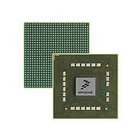
MPC8544VTALF Freescale Semiconductor, MPC8544VTALF Datasheet - Page 349

MPC8544VTALF
Manufacturer Part Number
MPC8544VTALF
Description
MPU POWERQUICC III 783-PBGA
Manufacturer
Freescale Semiconductor
Datasheets
1.MPC8544VTALF.pdf
(117 pages)
2.MPC8544VTALF.pdf
(2 pages)
3.MPC8544VTALF.pdf
(1340 pages)
Specifications of MPC8544VTALF
Processor Type
MPC85xx PowerQUICC III 32-Bit
Speed
667MHz
Voltage
1V
Mounting Type
Surface Mount
Package / Case
783-FCPBGA
Processor Series
MPC85xx
Core
e500
Data Bus Width
32 bit
Maximum Clock Frequency
667 MHz
Maximum Operating Temperature
+ 105 C
Mounting Style
SMD/SMT
Data Ram Size
32 KB
I/o Voltage
1.8 V, 3.3 V
Interface Type
I2C, HSSI, DUART
Minimum Operating Temperature
0 C
Lead Free Status / RoHS Status
Lead free / RoHS Compliant
Features
-
Lead Free Status / Rohs Status
Lead free / RoHS Compliant
Available stocks
Company
Part Number
Manufacturer
Quantity
Price
Company:
Part Number:
MPC8544VTALF
Manufacturer:
Freescale Semiconductor
Quantity:
10 000
Company:
Part Number:
MPC8544VTALFA
Manufacturer:
Freescale Semiconductor
Quantity:
10 000
- Current page: 349 of 1340
- Download datasheet (12Mb)
9.4.1.9
The DDR SDRAM mode configuration register, shown in
DDR’s mode registers.
Table 9-14
Freescale Semiconductor
28–31
16–31 SDMODE SDRAM mode. Specifies the initial value loaded into the DDR SDRAM mode register. The range of legal
0–15 ESDMODE Extended SDRAM mode. Specifies the initial value loaded into the DDR SDRAM extended mode register.
Bits
Bits
27
Offset 0x118
Reset
W
R
Name
0
D_INIT
describes the DDR_SDRAM_MODE fields.
Name
—
DDR SDRAM Mode Configuration (DDR_SDRAM_MODE)
MPC8544E PowerQUICC III Integrated Host Processor Family Reference Manual, Rev. 1
Figure 9-10. DDR SDRAM Mode Configuration Register (DDR_SDRAM_MODE)
The range and meaning of legal values is specified by the DDR SDRAM manufacturer.
When this value is driven onto the address bus (during the DDR SDRAM initialization sequence), MA[0]
presents the lsb of ESDMODE, which, in the big-endian convention shown in
ESDMODE[15]. The msb of the SDRAM extended mode register value must be stored at ESDMODE[0].
values is specified by the DDR SDRAM manufacturer.
When this value is driven onto the address bus (during DDR SDRAM initialization), MA[0] presents the lsb
of SDMODE, which, in the big-endian convention shown in
msb of the SDRAM mode register value must be stored at SDMODE[0]. Because the memory controller
forces SDMODE[7] to certain values depending on the state of the initialization sequence, (for resetting the
SDRAM’s DLL) the corresponding bits of this field are ignored by the memory controller. Note that
SDMODE[7] is mapped to MA[8].
Table 9-13. DDR_SDRAM_CFG_2 Field Descriptions (continued)
bit before the memory controller is enabled, the controller will automatically initialize DRAM after it is
enabled. This bit will be automatically cleared by hardware once the initialization is completed. This
data initialization bit should only be set when the controller is idle.
0 There is not data initialization in progress, and no data initialization is scheduled
1 The memory controller will initialize memory once it is enabled. This bit will remain asserted until
Reserved
DRAM data initialization This bit is set by software, and it is cleared by hardware. If software sets this
the initialization is complete. The value in DDR_DATA_INIT register will be used to initialize
memory.
Table 9-14. DDR_SDRAM_MODE Field Descriptions
ESDMODE
All zeros
15 16
Description
Description
Figure
Figure
9-10, sets the values loaded into the
9-10, corresponds to SDMODE[15]. The
SDMODE
Figure
Access: Read/Write
DDR Memory Controller
9-10, corresponds to
31
9-25
Related parts for MPC8544VTALF
Image
Part Number
Description
Manufacturer
Datasheet
Request
R
Part Number:
Description:
Manufacturer:
Freescale Semiconductor, Inc
Datasheet:
Part Number:
Description:
Manufacturer:
Freescale Semiconductor, Inc
Datasheet:
Part Number:
Description:
Manufacturer:
Freescale Semiconductor, Inc
Datasheet:
Part Number:
Description:
Manufacturer:
Freescale Semiconductor, Inc
Datasheet:
Part Number:
Description:
Manufacturer:
Freescale Semiconductor, Inc
Datasheet:
Part Number:
Description:
Manufacturer:
Freescale Semiconductor, Inc
Datasheet:
Part Number:
Description:
Manufacturer:
Freescale Semiconductor, Inc
Datasheet:
Part Number:
Description:
Manufacturer:
Freescale Semiconductor, Inc
Datasheet:
Part Number:
Description:
Manufacturer:
Freescale Semiconductor, Inc
Datasheet:
Part Number:
Description:
Manufacturer:
Freescale Semiconductor, Inc
Datasheet:
Part Number:
Description:
Manufacturer:
Freescale Semiconductor, Inc
Datasheet:
Part Number:
Description:
Manufacturer:
Freescale Semiconductor, Inc
Datasheet:
Part Number:
Description:
Manufacturer:
Freescale Semiconductor, Inc
Datasheet:
Part Number:
Description:
Manufacturer:
Freescale Semiconductor, Inc
Datasheet:
Part Number:
Description:
Manufacturer:
Freescale Semiconductor, Inc
Datasheet:


