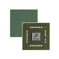
MPC8544VTALF Freescale Semiconductor, MPC8544VTALF Datasheet - Page 691

MPC8544VTALF
Manufacturer Part Number
MPC8544VTALF
Description
MPU POWERQUICC III 783-PBGA
Manufacturer
Freescale Semiconductor
Datasheets
1.MPC8544VTALF.pdf
(117 pages)
2.MPC8544VTALF.pdf
(2 pages)
3.MPC8544VTALF.pdf
(1340 pages)
Specifications of MPC8544VTALF
Processor Type
MPC85xx PowerQUICC III 32-Bit
Speed
667MHz
Voltage
1V
Mounting Type
Surface Mount
Package / Case
783-FCPBGA
Processor Series
MPC85xx
Core
e500
Data Bus Width
32 bit
Maximum Clock Frequency
667 MHz
Maximum Operating Temperature
+ 105 C
Mounting Style
SMD/SMT
Data Ram Size
32 KB
I/o Voltage
1.8 V, 3.3 V
Interface Type
I2C, HSSI, DUART
Minimum Operating Temperature
0 C
Lead Free Status / RoHS Status
Lead free / RoHS Compliant
Features
-
Lead Free Status / Rohs Status
Lead free / RoHS Compliant
Available stocks
Company
Part Number
Manufacturer
Quantity
Price
Company:
Part Number:
MPC8544VTALF
Manufacturer:
Freescale Semiconductor
Quantity:
10 000
Company:
Part Number:
MPC8544VTALFA
Manufacturer:
Freescale Semiconductor
Quantity:
10 000
- Current page: 691 of 1340
- Download datasheet (12Mb)
14.4.4.4.8
When a read access is handled by the UPM, and the UTA bit is 1 (data is to be sampled by the LBC), the
value of the DLT3 bit in the same RAM word, in conjunction with MxMR[GPLn4DIS], determines when
the data input is sampled by the LBC as follows:
Figure 14-61
14.4.4.4.9
When the LAST bit is read in a RAM word, the current UPM pattern is terminated at the end of the current
cycle. On the next cycle (following LAST) all the UPM signals are negated unconditionally (driven to
logic 1), unless there is a back-to-back UPM request pending. In this case, the signal values for the cycle
following the one in which the LAST bit was set are taken from the first RAM word of the pending UPM
routine.
14.4.4.4.10
The WAEN bit in the RAM array word can be used to enable the UPM wait mechanism in selected UPM
RAM words. If the UPM reads a RAM word with WAEN set, the external LUPWAIT signal is sampled
and synchronized by the memory controller as if it were an asynchronous signal. The WAEN bit is ignored
if LAST = 1 in the same RAM word.
Synchronization of LUPWAIT starts at the rising edge of the bus clock and takes at least 1 bus cycle to
complete. If LUPWAIT is asserted and WAEN = 1 in the current UPM word, the UPM is frozen until
LUPWAIT is negated. The value of external signals driven by the UPM remains as indicated in the
Freescale Semiconductor
•
•
To Internal
Data Bus
If MxMR[GPLn4DIS] = 1 (G4T4/DLT3 functions as DLT3) and DLT3 = 1 in the RAM word, data
is latched on the falling edge of the bus clock instead of the rising edge. The LBC samples the data
on the next falling edge of the bus clock, which is during the middle of the current bus cycle. This
feature should be used only in systems without external synchronous bus devices that require
mid-cycle sampling.
If GPLn4DIS = 0 (G4T4/DLT3 functions as G4T4), or if GPLn4DIS = 1 but DLT3 = 0, data is
latched on the rising edge of the bus clock, which occurs at the end of the current bus clock cycle
(normal operation).
shows how data sampling is controlled by the UPM.
MPC8544E PowerQUICC III Integrated Host Processor Family Reference Manual, Rev. 1
Data Valid and Data Sample Control (UTA)
LGPL[0:5] Signal Negation (LAST)
Wait Mechanism (WAEN)
Figure 14-61. UPM Read Access Data Sampling
UPM Read and GPL4nDIS = 1 and DLT3 = 1
1
0
LCLK
Local Bus Controller
LAD[0:31]
14-71
Related parts for MPC8544VTALF
Image
Part Number
Description
Manufacturer
Datasheet
Request
R
Part Number:
Description:
Manufacturer:
Freescale Semiconductor, Inc
Datasheet:
Part Number:
Description:
Manufacturer:
Freescale Semiconductor, Inc
Datasheet:
Part Number:
Description:
Manufacturer:
Freescale Semiconductor, Inc
Datasheet:
Part Number:
Description:
Manufacturer:
Freescale Semiconductor, Inc
Datasheet:
Part Number:
Description:
Manufacturer:
Freescale Semiconductor, Inc
Datasheet:
Part Number:
Description:
Manufacturer:
Freescale Semiconductor, Inc
Datasheet:
Part Number:
Description:
Manufacturer:
Freescale Semiconductor, Inc
Datasheet:
Part Number:
Description:
Manufacturer:
Freescale Semiconductor, Inc
Datasheet:
Part Number:
Description:
Manufacturer:
Freescale Semiconductor, Inc
Datasheet:
Part Number:
Description:
Manufacturer:
Freescale Semiconductor, Inc
Datasheet:
Part Number:
Description:
Manufacturer:
Freescale Semiconductor, Inc
Datasheet:
Part Number:
Description:
Manufacturer:
Freescale Semiconductor, Inc
Datasheet:
Part Number:
Description:
Manufacturer:
Freescale Semiconductor, Inc
Datasheet:
Part Number:
Description:
Manufacturer:
Freescale Semiconductor, Inc
Datasheet:
Part Number:
Description:
Manufacturer:
Freescale Semiconductor, Inc
Datasheet:


