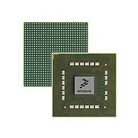
MPC8544VTALF Freescale Semiconductor, MPC8544VTALF Datasheet - Page 568

MPC8544VTALF
Manufacturer Part Number
MPC8544VTALF
Description
MPU POWERQUICC III 783-PBGA
Manufacturer
Freescale Semiconductor
Datasheets
1.MPC8544VTALF.pdf
(117 pages)
2.MPC8544VTALF.pdf
(2 pages)
3.MPC8544VTALF.pdf
(1340 pages)
Specifications of MPC8544VTALF
Processor Type
MPC85xx PowerQUICC III 32-Bit
Speed
667MHz
Voltage
1V
Mounting Type
Surface Mount
Package / Case
783-FCPBGA
Processor Series
MPC85xx
Core
e500
Data Bus Width
32 bit
Maximum Clock Frequency
667 MHz
Maximum Operating Temperature
+ 105 C
Mounting Style
SMD/SMT
Data Ram Size
32 KB
I/o Voltage
1.8 V, 3.3 V
Interface Type
I2C, HSSI, DUART
Minimum Operating Temperature
0 C
Lead Free Status / RoHS Status
Lead free / RoHS Compliant
Features
-
Lead Free Status / Rohs Status
Lead free / RoHS Compliant
Available stocks
Company
Part Number
Manufacturer
Quantity
Price
Company:
Part Number:
MPC8544VTALF
Manufacturer:
Freescale Semiconductor
Quantity:
10 000
Company:
Part Number:
MPC8544VTALFA
Manufacturer:
Freescale Semiconductor
Quantity:
10 000
- Current page: 568 of 1340
- Download datasheet (12Mb)
Security Engine (SEC) 2.1
12.4.7.10 KEU IV 1 Register (KEUIV1)
The KEUIV1 register is a general purpose IV register used during the initialization phase of the F8
algorithms for 3GPP, GSM A5/3, EDGE A5/3, GPRS GEA3 and also for the F9 algorithm for 3GPP. The
appropriate value as defined by the standards for each algorithm must be written before a new message is
started. After the initialization phase has been completed, KEUIV1 register is no longer used for the
remainder of F8 or F9 processing. However, if 3GPP F9, is selected, because the KEUIV1 register contains
the direction bit as defined by the 3GPP standard, the KEUIV1 register must be written back during
context switches, to complete the generation of the 3GPP MAC.
Address KEU 0x3_E100
12.4.7.11 KEU ICV_In Register (KEUICV)
If ICV checking is required, then the value to be compared with the computed F9 MAC value must be
written to the ICV_In register before data size is written.
12-88
16–23
24–25
27–31
31–63
Address KEU 0x3_E050
0–15
Bits
.
Reset
26
Reset
W
R
W
R
0
0
Name
CC
CA
CD
CB
CC
MPC8544E PowerQUICC III Integrated Host Processor Family Reference Manual, Rev. 1
0
It is the responsibility of the user to ensure that fields of the IV 1 register are
programmed correctly in accordance with the algorithm selected.
CC
Defined by the algorithm selected
Defined by the algorithm selected
Reserved
Defined by the algorithm selected (For 3GPP and GPRS, this is the communication direction bit)
Defined by the algorithm selected
Defined by the algorithm selected
15
Table 12-49. KEU IV_1 Register Field Descriptions
16
CA
Figure 12-65. KEU EU Go Register
Figure 12-66. KEU IV_1 Register
23
24
—
25
NOTE
CD
26
All zeros
All zeros
27
—
CB
Description
31
32
CC
Freescale Semiconductor
Access: Read/write
Access: Read/Write
63
63
Related parts for MPC8544VTALF
Image
Part Number
Description
Manufacturer
Datasheet
Request
R
Part Number:
Description:
Manufacturer:
Freescale Semiconductor, Inc
Datasheet:
Part Number:
Description:
Manufacturer:
Freescale Semiconductor, Inc
Datasheet:
Part Number:
Description:
Manufacturer:
Freescale Semiconductor, Inc
Datasheet:
Part Number:
Description:
Manufacturer:
Freescale Semiconductor, Inc
Datasheet:
Part Number:
Description:
Manufacturer:
Freescale Semiconductor, Inc
Datasheet:
Part Number:
Description:
Manufacturer:
Freescale Semiconductor, Inc
Datasheet:
Part Number:
Description:
Manufacturer:
Freescale Semiconductor, Inc
Datasheet:
Part Number:
Description:
Manufacturer:
Freescale Semiconductor, Inc
Datasheet:
Part Number:
Description:
Manufacturer:
Freescale Semiconductor, Inc
Datasheet:
Part Number:
Description:
Manufacturer:
Freescale Semiconductor, Inc
Datasheet:
Part Number:
Description:
Manufacturer:
Freescale Semiconductor, Inc
Datasheet:
Part Number:
Description:
Manufacturer:
Freescale Semiconductor, Inc
Datasheet:
Part Number:
Description:
Manufacturer:
Freescale Semiconductor, Inc
Datasheet:
Part Number:
Description:
Manufacturer:
Freescale Semiconductor, Inc
Datasheet:
Part Number:
Description:
Manufacturer:
Freescale Semiconductor, Inc
Datasheet:


