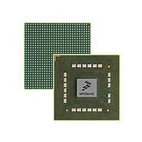
MPC8544VTALF Freescale Semiconductor, MPC8544VTALF Datasheet - Page 1237

MPC8544VTALF
Manufacturer Part Number
MPC8544VTALF
Description
MPU POWERQUICC III 783-PBGA
Manufacturer
Freescale Semiconductor
Datasheets
1.MPC8544VTALF.pdf
(117 pages)
2.MPC8544VTALF.pdf
(2 pages)
3.MPC8544VTALF.pdf
(1340 pages)
Specifications of MPC8544VTALF
Processor Type
MPC85xx PowerQUICC III 32-Bit
Speed
667MHz
Voltage
1V
Mounting Type
Surface Mount
Package / Case
783-FCPBGA
Processor Series
MPC85xx
Core
e500
Data Bus Width
32 bit
Maximum Clock Frequency
667 MHz
Maximum Operating Temperature
+ 105 C
Mounting Style
SMD/SMT
Data Ram Size
32 KB
I/o Voltage
1.8 V, 3.3 V
Interface Type
I2C, HSSI, DUART
Minimum Operating Temperature
0 C
Lead Free Status / RoHS Status
Lead free / RoHS Compliant
Features
-
Lead Free Status / Rohs Status
Lead free / RoHS Compliant
Available stocks
Company
Part Number
Manufacturer
Quantity
Price
Company:
Part Number:
MPC8544VTALF
Manufacturer:
Freescale Semiconductor
Quantity:
10 000
Company:
Part Number:
MPC8544VTALFA
Manufacturer:
Freescale Semiconductor
Quantity:
10 000
- Current page: 1237 of 1340
- Download datasheet (12Mb)
21.2.2
This section describes the details of the debug, watchpoint monitor, and JTAG test signals
21.2.2.1
Table 21-3
Freescale Semiconductor
MSRCID[0:4]
MECC[0:7]
MDVAL
Signal
describes all signals associated with device debug modes.
Detailed Signal Descriptions
Debug Signals—Details
MPC8544E PowerQUICC III Integrated Host Processor Family Reference Manual, Rev. 1
I/O
O Memory data-valid. Indicates when valid data is available. May be used by a logic analyzer to
O Memory ECC. DDR error checking and correcting. The normally bidirectional operation of the
O Memory source ID. Attribute signals associated with the memory interface that indicate the
capture the data on the data bus.
memory ECC (MECC) bus is described in
(ECC).”
In debug mode, the high-order 5 bits (MECC[0:4]) may be used to provide the transaction
source ID and MECC5 can be used as the data-valid indicator.
In debug mode, MECC[0:5] is constantly driven with debug information and must be
disconnected from the DDR memory’s ECC pins.
source ID for a transaction on an SDRAM interface. The SDRAM interface, DDR or local bus,
to which the debug information applies is specified during POR with MSRCID0 as shown in
Table
Meaning
Meaning
Meaning
Table 21-3. Debug Signals—Detailed Signal Descriptions
Timing Asserted/Negated—Referenced to the selected interface, (DDR or local bus).
Timing Driven every cycle in debug mode.
Timing Driven every cycle in debug mode. Similar timing to MA.
State
State
State
21-1. Two of these signals serve as reset configuration input signals.
This bus is used for debug functions when MSRCID1 is sampled low during POR.
Asserted—Indicates that data is valid on the data bus during the current clock cycle.
Asserted/Negated—In debug mode, MECC[0:5] is always driven. The source ID
Asserted/Negated—In debug mode, always driven with the value of the source ID.
When the DDR SDRAM interface is selected to source information on MDVAL,
this signal is valid for every cycle that data is driven or received on the DDR
SDRAM interface. When the LBC is selected, this signal is valid for every cycle
that data is driven or received on the local bus interface. The assertion of this
signal may be used by a logic analyzer to capture data.
Asserts when data is valid. Assertions are held for the duration of the transfer.
Read data timing is similar to MA. Write data timing is similar to the output
MDQ.
values appear during RAS and CAS cycles. A value of 0x1F (all ones) is driven
during cycles other than RAS and CAS. The data-valid indicator appears when
data is being received or driven on the pins.
The source ID has a value of 0x1F for cycles other than RAS and CAS. The
encodings shown in
transaction.
Table 21-26
Description
Section 9.5.11, “Error Checking and Correcting
provide detailed information about a memory
Debug Features and Watchpoint Facility
21-7
Related parts for MPC8544VTALF
Image
Part Number
Description
Manufacturer
Datasheet
Request
R
Part Number:
Description:
Manufacturer:
Freescale Semiconductor, Inc
Datasheet:
Part Number:
Description:
Manufacturer:
Freescale Semiconductor, Inc
Datasheet:
Part Number:
Description:
Manufacturer:
Freescale Semiconductor, Inc
Datasheet:
Part Number:
Description:
Manufacturer:
Freescale Semiconductor, Inc
Datasheet:
Part Number:
Description:
Manufacturer:
Freescale Semiconductor, Inc
Datasheet:
Part Number:
Description:
Manufacturer:
Freescale Semiconductor, Inc
Datasheet:
Part Number:
Description:
Manufacturer:
Freescale Semiconductor, Inc
Datasheet:
Part Number:
Description:
Manufacturer:
Freescale Semiconductor, Inc
Datasheet:
Part Number:
Description:
Manufacturer:
Freescale Semiconductor, Inc
Datasheet:
Part Number:
Description:
Manufacturer:
Freescale Semiconductor, Inc
Datasheet:
Part Number:
Description:
Manufacturer:
Freescale Semiconductor, Inc
Datasheet:
Part Number:
Description:
Manufacturer:
Freescale Semiconductor, Inc
Datasheet:
Part Number:
Description:
Manufacturer:
Freescale Semiconductor, Inc
Datasheet:
Part Number:
Description:
Manufacturer:
Freescale Semiconductor, Inc
Datasheet:
Part Number:
Description:
Manufacturer:
Freescale Semiconductor, Inc
Datasheet:


