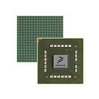
MPC8544VTALF Freescale Semiconductor, MPC8544VTALF Datasheet - Page 726

MPC8544VTALF
Manufacturer Part Number
MPC8544VTALF
Description
MPU POWERQUICC III 783-PBGA
Manufacturer
Freescale Semiconductor
Datasheets
1.MPC8544VTALF.pdf
(117 pages)
2.MPC8544VTALF.pdf
(2 pages)
3.MPC8544VTALF.pdf
(1340 pages)
Specifications of MPC8544VTALF
Processor Type
MPC85xx PowerQUICC III 32-Bit
Speed
667MHz
Voltage
1V
Mounting Type
Surface Mount
Package / Case
783-FCPBGA
Processor Series
MPC85xx
Core
e500
Data Bus Width
32 bit
Maximum Clock Frequency
667 MHz
Maximum Operating Temperature
+ 105 C
Mounting Style
SMD/SMT
Data Ram Size
32 KB
I/o Voltage
1.8 V, 3.3 V
Interface Type
I2C, HSSI, DUART
Minimum Operating Temperature
0 C
Lead Free Status / RoHS Status
Lead free / RoHS Compliant
Features
-
Lead Free Status / Rohs Status
Lead free / RoHS Compliant
Available stocks
Company
Part Number
Manufacturer
Quantity
Price
Company:
Part Number:
MPC8544VTALF
Manufacturer:
Freescale Semiconductor
Quantity:
10 000
Company:
Part Number:
MPC8544VTALFA
Manufacturer:
Freescale Semiconductor
Quantity:
10 000
- Current page: 726 of 1340
- Download datasheet (12Mb)
Local Bus Controller
This solution allows the local bus to react within multiple local bus clocks to the HTA signal and be still
within one DSI clock. Typically, LUPWAIT is synchronized internally, and only 2 clocks after LUPWAIT
changes, new data can be sampled or presented. For example, if the local bus clock ratio is 3× the DSI
clock, data can be sampled in the third local bus sub-clock, which is the last third of the DSI clock. If the
local bus clock ratio is only 2× the DSI clock, there is a special mode, where the LUPWAIT is NOT
synchronized. Refer to
Acknowledge,”
which is the second half of the DSI clock. AC timing of LUPWAIT must be met in this mode; otherwise
indeterministic behavior may occur.
The remaining issue is the synchronization of the UPM cycles to the beginning of the DSI clock cycle.
Because the UPM executes n cycles for every cycle of the DSI, a mechanism must be used to ensure that
the UPM changes transitions in a way that is synchronized to the DSI clock. The solution is to use a special
synchronize cycle at the beginning of the pattern. A GPL signal is used to control a multiplexer and to
activate external synchronization logic, which uses the DSI clock to stall the UPM by asserting LUPWAIT
until the beginning of the next DSI cycle. After that, this GPL signal must be negated and the multiplexer
connects LUPWAIT to HTA instead, for the rest of the bus cycle. Note that the GPL signals should be used
in the inverted state of their inactive state (GPL[0:4] are 1 when inactive, GPL5 is 0 when inactive) to start
the synchronization process.
14-106
MPC8544E PowerQUICC III Integrated Host Processor Family Reference Manual, Rev. 1
for more detailed information. In this mode, data is sampled in the second sub-clock,
Local Bus Interface
Figure 14-85. Interface to MSC8102 DSI in Synchronous Mode
Section 14.4.4.5, “Synchronous Sampling of LUPWAIT for Early Transfer
LUPWAIT
LAD[0:31]
LA[27:29]
LBS[0:3]
LGPL2
LGPL n
LGPLy
LCLK
LCS n
LALE
LCSy
INT n
Divider
Clock
Logic
Latch
Sync
HCLKIN
HTA
HD[0:31]
HA[11:26]
HCID[0:3]
HA[27:29]
HRDS/HRDE
HWBS/HDBS/
HWBE/HDBE[0:3]
HINT
HBRST
HBCS
HCS
MSC8102
Freescale Semiconductor
Related parts for MPC8544VTALF
Image
Part Number
Description
Manufacturer
Datasheet
Request
R
Part Number:
Description:
Manufacturer:
Freescale Semiconductor, Inc
Datasheet:
Part Number:
Description:
Manufacturer:
Freescale Semiconductor, Inc
Datasheet:
Part Number:
Description:
Manufacturer:
Freescale Semiconductor, Inc
Datasheet:
Part Number:
Description:
Manufacturer:
Freescale Semiconductor, Inc
Datasheet:
Part Number:
Description:
Manufacturer:
Freescale Semiconductor, Inc
Datasheet:
Part Number:
Description:
Manufacturer:
Freescale Semiconductor, Inc
Datasheet:
Part Number:
Description:
Manufacturer:
Freescale Semiconductor, Inc
Datasheet:
Part Number:
Description:
Manufacturer:
Freescale Semiconductor, Inc
Datasheet:
Part Number:
Description:
Manufacturer:
Freescale Semiconductor, Inc
Datasheet:
Part Number:
Description:
Manufacturer:
Freescale Semiconductor, Inc
Datasheet:
Part Number:
Description:
Manufacturer:
Freescale Semiconductor, Inc
Datasheet:
Part Number:
Description:
Manufacturer:
Freescale Semiconductor, Inc
Datasheet:
Part Number:
Description:
Manufacturer:
Freescale Semiconductor, Inc
Datasheet:
Part Number:
Description:
Manufacturer:
Freescale Semiconductor, Inc
Datasheet:
Part Number:
Description:
Manufacturer:
Freescale Semiconductor, Inc
Datasheet:


