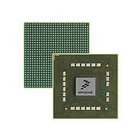
MPC8544VTALF Freescale Semiconductor, MPC8544VTALF Datasheet - Page 213

MPC8544VTALF
Manufacturer Part Number
MPC8544VTALF
Description
MPU POWERQUICC III 783-PBGA
Manufacturer
Freescale Semiconductor
Datasheets
1.MPC8544VTALF.pdf
(117 pages)
2.MPC8544VTALF.pdf
(2 pages)
3.MPC8544VTALF.pdf
(1340 pages)
Specifications of MPC8544VTALF
Processor Type
MPC85xx PowerQUICC III 32-Bit
Speed
667MHz
Voltage
1V
Mounting Type
Surface Mount
Package / Case
783-FCPBGA
Processor Series
MPC85xx
Core
e500
Data Bus Width
32 bit
Maximum Clock Frequency
667 MHz
Maximum Operating Temperature
+ 105 C
Mounting Style
SMD/SMT
Data Ram Size
32 KB
I/o Voltage
1.8 V, 3.3 V
Interface Type
I2C, HSSI, DUART
Minimum Operating Temperature
0 C
Lead Free Status / RoHS Status
Lead free / RoHS Compliant
Features
-
Lead Free Status / Rohs Status
Lead free / RoHS Compliant
Available stocks
Company
Part Number
Manufacturer
Quantity
Price
Company:
Part Number:
MPC8544VTALF
Manufacturer:
Freescale Semiconductor
Quantity:
10 000
Company:
Part Number:
MPC8544VTALFA
Manufacturer:
Freescale Semiconductor
Quantity:
10 000
- Current page: 213 of 1340
- Download datasheet (12Mb)
instruction establishes a reservation and is paired with a store conditional instruction to achieve the atomic
operation. However, there are restrictions and requirements for this functionality. The processor revokes
reservations during a context switch, so the programmer must reacquire the reservation after a context
switch occurs.
5.10.2
The core complex supports weakly ordered references to memory. Thus the e500 manages the order and
synchronization of instructions to ensure proper execution when memory is shared between multiple
processes or programs. The cache and data memory control attributes, along with msync and mbar,
provide the required access control.
5.10.3
The core complex supports instructions for performing a full range of cache control functions, including
cache locking by line. The core complex supports broadcasting and snooping of these cache control
instructions on the CCB. The e500 core also supports the following e500-specific cache locking
instructions:
5.10.4
Cache and memory attributes are programmable on a per-page basis. In addition to the write-through,
caching-inhibited, memory coherency enforced, and guarded characteristics defined by the WIMG bits,
the endianness bit, E, allows selection of big- or little-endian byte ordering on a per-page basis.
In addition to the WIMGE bits, the MMU model defines user-definable page attribute bits U0–U3.
5.11
The core complex defines a versatile local bus interface that allows a wide range of system performance
and system-complexity trade-offs. The interface defines the following buses:
Two of the data buses are general-purpose data-in buses for reads, and the third is a data-out bus for writes.
The two data-in buses feature support for out-of-order read transactions from two different sources
simultaneously, and all three data buses may be operated concurrently. The address-in bus supports
snooping for external management of the L1 caches and TLBs by other bus masters. The core complex
Freescale Semiconductor
•
•
•
•
•
•
•
•
Data Cache Block Lock Clear (dcblc)
Data Cache Block Touch and Lock Set (dcbtls)
Data Cache Block Touch for Store and Lock Set (dcbtstls)
Instruction Cache Block Lock Clear (icblc)
Instruction Cache Block Touch and Lock Set (icbtls)
An address-out bus for mastering bus transactions
An address-in bus for snooping internal resources
Three tagged data buses
Core Complex Bus (CCB)
Memory Access Ordering
Cache Control Instructions
Programmable Page Characteristics
MPC8544E PowerQUICC III Integrated Host Processor Family Reference Manual, Rev. 1
Core Complex Overview
5-27
Related parts for MPC8544VTALF
Image
Part Number
Description
Manufacturer
Datasheet
Request
R
Part Number:
Description:
Manufacturer:
Freescale Semiconductor, Inc
Datasheet:
Part Number:
Description:
Manufacturer:
Freescale Semiconductor, Inc
Datasheet:
Part Number:
Description:
Manufacturer:
Freescale Semiconductor, Inc
Datasheet:
Part Number:
Description:
Manufacturer:
Freescale Semiconductor, Inc
Datasheet:
Part Number:
Description:
Manufacturer:
Freescale Semiconductor, Inc
Datasheet:
Part Number:
Description:
Manufacturer:
Freescale Semiconductor, Inc
Datasheet:
Part Number:
Description:
Manufacturer:
Freescale Semiconductor, Inc
Datasheet:
Part Number:
Description:
Manufacturer:
Freescale Semiconductor, Inc
Datasheet:
Part Number:
Description:
Manufacturer:
Freescale Semiconductor, Inc
Datasheet:
Part Number:
Description:
Manufacturer:
Freescale Semiconductor, Inc
Datasheet:
Part Number:
Description:
Manufacturer:
Freescale Semiconductor, Inc
Datasheet:
Part Number:
Description:
Manufacturer:
Freescale Semiconductor, Inc
Datasheet:
Part Number:
Description:
Manufacturer:
Freescale Semiconductor, Inc
Datasheet:
Part Number:
Description:
Manufacturer:
Freescale Semiconductor, Inc
Datasheet:
Part Number:
Description:
Manufacturer:
Freescale Semiconductor, Inc
Datasheet:


