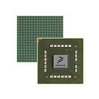
MPC8544VTALF Freescale Semiconductor, MPC8544VTALF Datasheet - Page 392

MPC8544VTALF
Manufacturer Part Number
MPC8544VTALF
Description
MPU POWERQUICC III 783-PBGA
Manufacturer
Freescale Semiconductor
Datasheets
1.MPC8544VTALF.pdf
(117 pages)
2.MPC8544VTALF.pdf
(2 pages)
3.MPC8544VTALF.pdf
(1340 pages)
Specifications of MPC8544VTALF
Processor Type
MPC85xx PowerQUICC III 32-Bit
Speed
667MHz
Voltage
1V
Mounting Type
Surface Mount
Package / Case
783-FCPBGA
Processor Series
MPC85xx
Core
e500
Data Bus Width
32 bit
Maximum Clock Frequency
667 MHz
Maximum Operating Temperature
+ 105 C
Mounting Style
SMD/SMT
Data Ram Size
32 KB
I/o Voltage
1.8 V, 3.3 V
Interface Type
I2C, HSSI, DUART
Minimum Operating Temperature
0 C
Lead Free Status / RoHS Status
Lead free / RoHS Compliant
Features
-
Lead Free Status / Rohs Status
Lead free / RoHS Compliant
Available stocks
Company
Part Number
Manufacturer
Quantity
Price
Company:
Part Number:
MPC8544VTALF
Manufacturer:
Freescale Semiconductor
Quantity:
10 000
Company:
Part Number:
MPC8544VTALFA
Manufacturer:
Freescale Semiconductor
Quantity:
10 000
- Current page: 392 of 1340
- Download datasheet (12Mb)
DDR Memory Controller
9.6
System software must configure the DDR memory controller, using a memory polling algorithm at system
start-up, to correctly map the size of each bank in memory. Then, the DDR memory controller uses its bank
map to assert the appropriate MCSn signal for memory accesses according to the provided bank depths.
System software must also configure the DDR memory controller at system start-up to appropriately
multiplex the row and column address bits for each bank. Refer to row-address configuration in
Section 9.4.1.2, “Chip Select Configuration (CSn_CONFIG).”
these configuration bits.
At system reset, initialization software (boot code) must set up the programmable parameters in the
memory interface configuration registers. See
descriptions of the configuration registers. These parameters are shown in
9-68
Access Error
Notification
Category
TIMING_CFG_3
TIMING_CFG_0
TIMING_CFG_1
TIMING_CFG_2
CSn_CONFIG
CSn_BNDS
Initialization/Application Information
Name
MPC8544E PowerQUICC III Integrated Host Processor Family Reference Manual, Rev. 1
Single-bit ECC
threshold
Multi-bit ECC
error
Memory select
error
Table 9-53. Memory Interface Configuration Register Initialization Parameters
Error
Chip select memory bounds
Chip select configuration
Extended timing parameters for fields
in TIMING_CFG_1
Timing configuration
Timing configuration
Timing configuration
The number of ECC errors has reached the
threshold specified in the ERR_SBE.
A multi-bit ECC error is detected during a read, or
read-modify-write memory operation.
Read, or write, address does not fall within the
address range of any of the memory banks.
Table 9-52. Memory Controller Errors
Description
Descriptions
Section 9.4.1, “Register Descriptions,”
ODT_WR_CFG
ODT_RD_CFG
RD_TO_PRE
PRETOACT
ACTTOPRE
ACTTORW
CS_n_EN
AP_n_EN
ADD_LAT
WR_LAT
CASLAT
Address multiplexing occurs according to
WWT
RWT
WRT
CPO
RRT
EXT_REFREC
Parameter
The error is reported
via machine check
or critical interrupt if
enabled.
SAn
EAn
Table
WR_DATA_DELAY
ROW_BITS_CS_n
COL_BITS_CS_n
Action
BA_BITS_CS_n
PRE_PD_EXIT
ODT_PD_EXIT
ACT_PD_EXIT
FOUR_ACT
ACTTOACT
MRS_CYC
CKE_PLS
WRTORD
REFREC
WRREC
9-53.
Freescale Semiconductor
for more detailed
The error control
register only logs
read versus write,
not full type
Detect Register
Section/page
9.4.1.1/9-11
9.4.1.2/9-11
9.4.1.3/9-13
9.4.1.4/9-14
9.4.1.5/9-16
9.4.1.6/9-18
Related parts for MPC8544VTALF
Image
Part Number
Description
Manufacturer
Datasheet
Request
R
Part Number:
Description:
Manufacturer:
Freescale Semiconductor, Inc
Datasheet:
Part Number:
Description:
Manufacturer:
Freescale Semiconductor, Inc
Datasheet:
Part Number:
Description:
Manufacturer:
Freescale Semiconductor, Inc
Datasheet:
Part Number:
Description:
Manufacturer:
Freescale Semiconductor, Inc
Datasheet:
Part Number:
Description:
Manufacturer:
Freescale Semiconductor, Inc
Datasheet:
Part Number:
Description:
Manufacturer:
Freescale Semiconductor, Inc
Datasheet:
Part Number:
Description:
Manufacturer:
Freescale Semiconductor, Inc
Datasheet:
Part Number:
Description:
Manufacturer:
Freescale Semiconductor, Inc
Datasheet:
Part Number:
Description:
Manufacturer:
Freescale Semiconductor, Inc
Datasheet:
Part Number:
Description:
Manufacturer:
Freescale Semiconductor, Inc
Datasheet:
Part Number:
Description:
Manufacturer:
Freescale Semiconductor, Inc
Datasheet:
Part Number:
Description:
Manufacturer:
Freescale Semiconductor, Inc
Datasheet:
Part Number:
Description:
Manufacturer:
Freescale Semiconductor, Inc
Datasheet:
Part Number:
Description:
Manufacturer:
Freescale Semiconductor, Inc
Datasheet:
Part Number:
Description:
Manufacturer:
Freescale Semiconductor, Inc
Datasheet:


