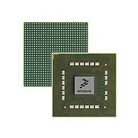
MPC8544VTALF Freescale Semiconductor, MPC8544VTALF Datasheet - Page 705

MPC8544VTALF
Manufacturer Part Number
MPC8544VTALF
Description
MPU POWERQUICC III 783-PBGA
Manufacturer
Freescale Semiconductor
Datasheets
1.MPC8544VTALF.pdf
(117 pages)
2.MPC8544VTALF.pdf
(2 pages)
3.MPC8544VTALF.pdf
(1340 pages)
Specifications of MPC8544VTALF
Processor Type
MPC85xx PowerQUICC III 32-Bit
Speed
667MHz
Voltage
1V
Mounting Type
Surface Mount
Package / Case
783-FCPBGA
Processor Series
MPC85xx
Core
e500
Data Bus Width
32 bit
Maximum Clock Frequency
667 MHz
Maximum Operating Temperature
+ 105 C
Mounting Style
SMD/SMT
Data Ram Size
32 KB
I/o Voltage
1.8 V, 3.3 V
Interface Type
I2C, HSSI, DUART
Minimum Operating Temperature
0 C
Lead Free Status / RoHS Status
Lead free / RoHS Compliant
Features
-
Lead Free Status / Rohs Status
Lead free / RoHS Compliant
Available stocks
Company
Part Number
Manufacturer
Quantity
Price
Company:
Part Number:
MPC8544VTALF
Manufacturer:
Freescale Semiconductor
Quantity:
10 000
Company:
Part Number:
MPC8544VTALFA
Manufacturer:
Freescale Semiconductor
Quantity:
10 000
- Current page: 705 of 1340
- Download datasheet (12Mb)
14.5.4
The following sections provide application information on interfacing to SDRAM.
14.5.4.1
The LBC provides one SDRAM machine for the local bus. Although there is only one machine, multiple
chip selects (LCSn) can be programmed to support multiple SDRAM devices. Note that no limitation
exists on the number of chip selects that can be programmed for SDRAM. This means that LCS[1:7] can
be programmed to support SDRAM, assuming LCS0 is reserved for the GPCM to connect to Flash
memory.
If multiple chip selects are configured to support SDRAM on the local bus, each SDRAM device should
have the same port size and timing parameters. This means that all option registers (ORn) for the SDRAM
chip selects should be programmed exactly the same.
All the chip selects share the same local bus SDRAM mode register (LSDMR) for initialization along with
the local bus-assigned SDRAM refresh timer register (LSRT) and the memory refresh timer prescaler
register (MPTPR) for refresh.
Freescale Semiconductor
1
2
3
Half word
Transfer
Address state is the calculated address for port size.
OP n : These lanes are read or written during that bus transaction. OP0 is the most-significant byte of
a word operand and OP3 is the least-significant byte.
— Denotes a byte not driven during that write cycle.
Word
Size
Interfacing to SDRAM
MPC8544E PowerQUICC III Integrated Host Processor Family Reference Manual, Rev. 1
Basic SDRAM Capabilities of the Local Bus
Although in principle it is possible to mix different port sizes and timing
parameters, combinations are limited and this operation is not
recommended.
Table 14-31. Data Bus Requirements For Read Cycle (continued)
Address
A[29:31]
State
000
001
010
100
101
110
000
100
1
OP0
OP4
OP0
OP4
0–7
—
—
—
—
8–15
OP1
OP1
OP5
OP5
OP1
OP5
—
—
32-Bit
NOTE
Port Size/Data Bus Assignments
16–23
OP2
OP2
OP6
OP6
OP2
OP6
—
—
24–31
OP3
OP7
OP3
OP7
—
—
—
—
OP0
OP2
OP4
OP6
OP0
OP4
0–7
—
—
16-Bit
8–15
OP1
OP1
OP3
OP5
OP5
OP7
OP1
OP5
Local Bus Controller
8-Bit
OP0
OP1
OP2
OP4
OP5
OP6
OP0
OP4
0–7
14-85
Related parts for MPC8544VTALF
Image
Part Number
Description
Manufacturer
Datasheet
Request
R
Part Number:
Description:
Manufacturer:
Freescale Semiconductor, Inc
Datasheet:
Part Number:
Description:
Manufacturer:
Freescale Semiconductor, Inc
Datasheet:
Part Number:
Description:
Manufacturer:
Freescale Semiconductor, Inc
Datasheet:
Part Number:
Description:
Manufacturer:
Freescale Semiconductor, Inc
Datasheet:
Part Number:
Description:
Manufacturer:
Freescale Semiconductor, Inc
Datasheet:
Part Number:
Description:
Manufacturer:
Freescale Semiconductor, Inc
Datasheet:
Part Number:
Description:
Manufacturer:
Freescale Semiconductor, Inc
Datasheet:
Part Number:
Description:
Manufacturer:
Freescale Semiconductor, Inc
Datasheet:
Part Number:
Description:
Manufacturer:
Freescale Semiconductor, Inc
Datasheet:
Part Number:
Description:
Manufacturer:
Freescale Semiconductor, Inc
Datasheet:
Part Number:
Description:
Manufacturer:
Freescale Semiconductor, Inc
Datasheet:
Part Number:
Description:
Manufacturer:
Freescale Semiconductor, Inc
Datasheet:
Part Number:
Description:
Manufacturer:
Freescale Semiconductor, Inc
Datasheet:
Part Number:
Description:
Manufacturer:
Freescale Semiconductor, Inc
Datasheet:
Part Number:
Description:
Manufacturer:
Freescale Semiconductor, Inc
Datasheet:


