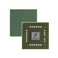
MPC8544VTALF Freescale Semiconductor, MPC8544VTALF Datasheet - Page 660

MPC8544VTALF
Manufacturer Part Number
MPC8544VTALF
Description
MPU POWERQUICC III 783-PBGA
Manufacturer
Freescale Semiconductor
Datasheets
1.MPC8544VTALF.pdf
(117 pages)
2.MPC8544VTALF.pdf
(2 pages)
3.MPC8544VTALF.pdf
(1340 pages)
Specifications of MPC8544VTALF
Processor Type
MPC85xx PowerQUICC III 32-Bit
Speed
667MHz
Voltage
1V
Mounting Type
Surface Mount
Package / Case
783-FCPBGA
Processor Series
MPC85xx
Core
e500
Data Bus Width
32 bit
Maximum Clock Frequency
667 MHz
Maximum Operating Temperature
+ 105 C
Mounting Style
SMD/SMT
Data Ram Size
32 KB
I/o Voltage
1.8 V, 3.3 V
Interface Type
I2C, HSSI, DUART
Minimum Operating Temperature
0 C
Lead Free Status / RoHS Status
Lead free / RoHS Compliant
Features
-
Lead Free Status / Rohs Status
Lead free / RoHS Compliant
Available stocks
Company
Part Number
Manufacturer
Quantity
Price
Company:
Part Number:
MPC8544VTALF
Manufacturer:
Freescale Semiconductor
Quantity:
10 000
Company:
Part Number:
MPC8544VTALFA
Manufacturer:
Freescale Semiconductor
Quantity:
10 000
- Current page: 660 of 1340
- Download datasheet (12Mb)
Local Bus Controller
The timing diagram in
14.4.2.2.1
The GPCM supports internal generation of transfer acknowledge. It allows between zero and 30 wait states
to be added to an access by programming ORn[SCY] and ORn[TRLX]. Internal generation of transfer
acknowledge is enabled if ORn[SETA] = 0. If LGTA is asserted externally two bus clock cycles or more
before the wait state counter has expired (to allow for synchronization latency), the current memory cycle
is terminated by LGTA; otherwise it is terminated by the expiration of the wait state counter. Regardless
of the setting of ORn[SETA], wait states prolong the assertion duration of both LOE and LWEn in the same
manner. When TRLX = 1, the number of wait states inserted by the memory controller is doubled from
ORn[SCY] cycles to 2 × ORn[SCY] cycles, allowing a maximum of 30 wait states.
14.4.2.2.2
Figure 14-23
LCSn is connected directly to CE of the memory device. The LWE[0:3] signals are connected to the
respective WE[3:0] signals on the memory device where each LWE[0:3] signal corresponds to a different
data byte.
As
transaction are supplied by LOE or LWEn, depending on the transaction direction—read or write (write case
shown in
14-40
Figure 14-25
•
•
•
•
•
One quarter of a clock cycle later.
One half of a clock cycle later
One clock cycle later (for LCRR[CLKDIV] = 2 (clock ratio of 4)) when ORn[XACS] = 1.
Two clock cycles later, when ORn[XACS] = 1.
Three clock cycles later, when ORn[XACS] = 1 and ORn[TRLX] = 1.
Figure
LWE n
LCLK
LALE
LCS n
Figure 14-25. GPCM Basic Write Timing (XACS = 0, ACS = 00, CSNT = 1, SCY = 1,
LAD
LOE
shows a basic connection between the local bus and a static memory device. In this case,
MPC8544E PowerQUICC III Integrated Host Processor Family Reference Manual, Rev. 1
TA
A
14-25). ORn[CSNT] controls the timing for the appropriate strobe negation in write cycles.
Programmable Wait State Configuration
Chip-Select and Write Enable Negation Timing
shows, the timing for LCSn is the same as for the latched address. The strobes for the
Address
Figure 14-24
shows two chip-select assertion timings.
TRLX = 0)
Latched Address
SCY = 1
Write Data
CSNT = 1
Freescale Semiconductor
Related parts for MPC8544VTALF
Image
Part Number
Description
Manufacturer
Datasheet
Request
R
Part Number:
Description:
Manufacturer:
Freescale Semiconductor, Inc
Datasheet:
Part Number:
Description:
Manufacturer:
Freescale Semiconductor, Inc
Datasheet:
Part Number:
Description:
Manufacturer:
Freescale Semiconductor, Inc
Datasheet:
Part Number:
Description:
Manufacturer:
Freescale Semiconductor, Inc
Datasheet:
Part Number:
Description:
Manufacturer:
Freescale Semiconductor, Inc
Datasheet:
Part Number:
Description:
Manufacturer:
Freescale Semiconductor, Inc
Datasheet:
Part Number:
Description:
Manufacturer:
Freescale Semiconductor, Inc
Datasheet:
Part Number:
Description:
Manufacturer:
Freescale Semiconductor, Inc
Datasheet:
Part Number:
Description:
Manufacturer:
Freescale Semiconductor, Inc
Datasheet:
Part Number:
Description:
Manufacturer:
Freescale Semiconductor, Inc
Datasheet:
Part Number:
Description:
Manufacturer:
Freescale Semiconductor, Inc
Datasheet:
Part Number:
Description:
Manufacturer:
Freescale Semiconductor, Inc
Datasheet:
Part Number:
Description:
Manufacturer:
Freescale Semiconductor, Inc
Datasheet:
Part Number:
Description:
Manufacturer:
Freescale Semiconductor, Inc
Datasheet:
Part Number:
Description:
Manufacturer:
Freescale Semiconductor, Inc
Datasheet:


