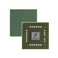
MPC8544VTALF Freescale Semiconductor, MPC8544VTALF Datasheet - Page 622

MPC8544VTALF
Manufacturer Part Number
MPC8544VTALF
Description
MPU POWERQUICC III 783-PBGA
Manufacturer
Freescale Semiconductor
Datasheets
1.MPC8544VTALF.pdf
(117 pages)
2.MPC8544VTALF.pdf
(2 pages)
3.MPC8544VTALF.pdf
(1340 pages)
Specifications of MPC8544VTALF
Processor Type
MPC85xx PowerQUICC III 32-Bit
Speed
667MHz
Voltage
1V
Mounting Type
Surface Mount
Package / Case
783-FCPBGA
Processor Series
MPC85xx
Core
e500
Data Bus Width
32 bit
Maximum Clock Frequency
667 MHz
Maximum Operating Temperature
+ 105 C
Mounting Style
SMD/SMT
Data Ram Size
32 KB
I/o Voltage
1.8 V, 3.3 V
Interface Type
I2C, HSSI, DUART
Minimum Operating Temperature
0 C
Lead Free Status / RoHS Status
Lead free / RoHS Compliant
Features
-
Lead Free Status / Rohs Status
Lead free / RoHS Compliant
Available stocks
Company
Part Number
Manufacturer
Quantity
Price
Company:
Part Number:
MPC8544VTALF
Manufacturer:
Freescale Semiconductor
Quantity:
10 000
Company:
Part Number:
MPC8544VTALFA
Manufacturer:
Freescale Semiconductor
Quantity:
10 000
- Current page: 622 of 1340
- Download datasheet (12Mb)
Local Bus Controller
14.1.1
The main component of the LBC is its memory controller, which provides a seamless interface to many
types of memory devices and peripherals. The memory controller is responsible for controlling eight
memory banks shared by a high performance SDRAM machine, a GPCM, and up to three UPMs. As such,
it supports a minimal glue logic interface to synchronous DRAM (SDRAM), SRAM, EPROM, Flash
EPROM, burstable RAM, regular DRAM devices, extended data output DRAM devices, and other
peripherals. The external address latch signal (LALE) allows multiplexing of addresses with data signals
to reduce the device signal count.
The LBC also includes a number of data checking and protection features such as data parity generation
and checking, write protection and a bus monitor to ensure that each bus cycle is terminated within a
user-specified period.
14.1.2
The LBC main features are as follows:
1. Refers to the logical address space of the LBC. Once the address is decoded by the LBC,
right-most 34 bits of the 36-bit physical address space.
14-2
•
•
•
Memory controller with eight memory banks
— 34-bit
— Variable memory block sizes (32 Kbytes to 4 Gbytes)
— Selection of control signal generation on a per-bank basis
— Data buffer controls activated on a per-bank basis
— Up to 256-byte bursts, arbitrarily aligned
— Automatic segmentation of large transactions
— Odd/even parity checking including read-modify-write (RMW) parity for single accesses
— Write-protection capability
— Atomic operation
— Parity byte-select
SDRAM machine
— Provides the control functions and signals for glueless connection to JEDEC-compliant
— Supports up to four concurrent open pages per device
— Supports SDRAM port size of 32, 16, and 8 bits
— Supports external address and/or command lines buffering
General-purpose chip-select machine (GPCM)
— Compatible with SRAM, EPROM, FEPROM, and peripherals
— Global (boot) chip-select available at system reset
— Boot chip-select support for 8-, 16-, 32-bit devices
— Minimum 3-clock access to external devices
SDRAM devices
Overview
Features
MPC8544E PowerQUICC III Integrated Host Processor Family Reference Manual, Rev. 1
1
address decoding with mask
the 34-bit address becomes the
Freescale Semiconductor
Related parts for MPC8544VTALF
Image
Part Number
Description
Manufacturer
Datasheet
Request
R
Part Number:
Description:
Manufacturer:
Freescale Semiconductor, Inc
Datasheet:
Part Number:
Description:
Manufacturer:
Freescale Semiconductor, Inc
Datasheet:
Part Number:
Description:
Manufacturer:
Freescale Semiconductor, Inc
Datasheet:
Part Number:
Description:
Manufacturer:
Freescale Semiconductor, Inc
Datasheet:
Part Number:
Description:
Manufacturer:
Freescale Semiconductor, Inc
Datasheet:
Part Number:
Description:
Manufacturer:
Freescale Semiconductor, Inc
Datasheet:
Part Number:
Description:
Manufacturer:
Freescale Semiconductor, Inc
Datasheet:
Part Number:
Description:
Manufacturer:
Freescale Semiconductor, Inc
Datasheet:
Part Number:
Description:
Manufacturer:
Freescale Semiconductor, Inc
Datasheet:
Part Number:
Description:
Manufacturer:
Freescale Semiconductor, Inc
Datasheet:
Part Number:
Description:
Manufacturer:
Freescale Semiconductor, Inc
Datasheet:
Part Number:
Description:
Manufacturer:
Freescale Semiconductor, Inc
Datasheet:
Part Number:
Description:
Manufacturer:
Freescale Semiconductor, Inc
Datasheet:
Part Number:
Description:
Manufacturer:
Freescale Semiconductor, Inc
Datasheet:
Part Number:
Description:
Manufacturer:
Freescale Semiconductor, Inc
Datasheet:


