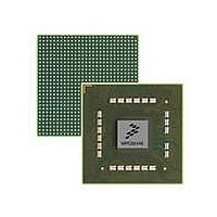
MPC8544VTALF Freescale Semiconductor, MPC8544VTALF Datasheet - Page 740

MPC8544VTALF
Manufacturer Part Number
MPC8544VTALF
Description
MPU POWERQUICC III 783-PBGA
Manufacturer
Freescale Semiconductor
Datasheets
1.MPC8544VTALF.pdf
(117 pages)
2.MPC8544VTALF.pdf
(2 pages)
3.MPC8544VTALF.pdf
(1340 pages)
Specifications of MPC8544VTALF
Processor Type
MPC85xx PowerQUICC III 32-Bit
Speed
667MHz
Voltage
1V
Mounting Type
Surface Mount
Package / Case
783-FCPBGA
Processor Series
MPC85xx
Core
e500
Data Bus Width
32 bit
Maximum Clock Frequency
667 MHz
Maximum Operating Temperature
+ 105 C
Mounting Style
SMD/SMT
Data Ram Size
32 KB
I/o Voltage
1.8 V, 3.3 V
Interface Type
I2C, HSSI, DUART
Minimum Operating Temperature
0 C
Lead Free Status / RoHS Status
Lead free / RoHS Compliant
Features
-
Lead Free Status / Rohs Status
Lead free / RoHS Compliant
Available stocks
Company
Part Number
Manufacturer
Quantity
Price
Company:
Part Number:
MPC8544VTALF
Manufacturer:
Freescale Semiconductor
Quantity:
10 000
Company:
Part Number:
MPC8544VTALFA
Manufacturer:
Freescale Semiconductor
Quantity:
10 000
- Current page: 740 of 1340
- Download datasheet (12Mb)
Enhanced Three-Speed Ethernet Controllers
15.4.1
Below is a description of the eTSEC interface signals. For RGMII mode details please refer to the
Hewlett-Packard reduced gigabit media-independent interface (RGMII) specification version 1.2a, dated
9/22/2000. RMII mode details follow the RMII Consortium Specification, dated 3/20/1998. All other
modes follow the IEEE 802.3 standard, 2000 Edition. Input signals not used are internally disabled. Except
for TSECn_GTX_CLK, output signals not used are driven low.
15-8
TSEC n _TXD[7:4]
TSEC n _TXD[3:0]
TSEC n _TX_CLK
SD2_REF_CLK,
TSEC n _TX_ER
TSEC n _TX_EN
SD2_REF_CLK
SD2_RX[ n-1 ],
Signal Name
SD2_TX[ n-1 ],
SD2_RX[ n-1 ]
SD2_TX[ n-1 ]
Detailed Signal Descriptions
MPC8544E PowerQUICC III Integrated Host Processor Family Reference Manual, Rev. 1
Table 15-1. eTSEC n Network Interface Signal Properties (continued)
MII—transmit clock, input
TBI—PMA receive clock 1, input
RMII—reference transmit and receive clock, input
FIFO—transmit clock, input
RGMII, RTBI—unused
GMII—transmit data bit 7:4, output
TBI—transmit code group (TCG) bit 7:4, output
FIFO—transmit data bit 7:4, output
MII, RGMII, RTBI, RMII—unused, output driven zero
GMII, MII—Transmit data bits 3:0, output
TBI—TCG bits 3:0, output
RGMII (TX_CLK rising)—Transmit data bits 3:0, output
RGMII (TX_CLK falling)—Transmit data bits 7:4, output
RTBI (TX_CLK rising)—TCG bits 3:0, output
RTBI (TX_CLK falling)—TCG bits 8:5, output
RMII—TXD[1:0] transmit data bits, output
RMII—TXD[3:2] unused, output driven zeroFIFO—Transmit data bits 3:0, output
GMII, MII—transmit error, output
RGMII, RTBI, RMII—unused, output driven zero
TBI—TCG bit 9, output
FIFO—transmit error or transmit frame control bit, output
GMII, MII, RMII—Transmit data valid, output
TBI—TCG bit 8, output
RGMII (TX_CLK rising)—Transmit data enabled, output
RGMII (TX_CLK falling)—Transmit error, output
RTBI (TX_CLK rising)—TCG bit 4, output
RTBI (TX_CLK falling)—TCG bit 9, output
FIFO—Transmit data valid or transmit control bit, output
SGMII transmit data (and complement)
SGMII receive data (and complement)
SGMII SerDes2 PLL reference clock (and complement)
Function
Freescale Semiconductor
Reset
State
0000
0000
—
—
—
—
0
0
Related parts for MPC8544VTALF
Image
Part Number
Description
Manufacturer
Datasheet
Request
R
Part Number:
Description:
Manufacturer:
Freescale Semiconductor, Inc
Datasheet:
Part Number:
Description:
Manufacturer:
Freescale Semiconductor, Inc
Datasheet:
Part Number:
Description:
Manufacturer:
Freescale Semiconductor, Inc
Datasheet:
Part Number:
Description:
Manufacturer:
Freescale Semiconductor, Inc
Datasheet:
Part Number:
Description:
Manufacturer:
Freescale Semiconductor, Inc
Datasheet:
Part Number:
Description:
Manufacturer:
Freescale Semiconductor, Inc
Datasheet:
Part Number:
Description:
Manufacturer:
Freescale Semiconductor, Inc
Datasheet:
Part Number:
Description:
Manufacturer:
Freescale Semiconductor, Inc
Datasheet:
Part Number:
Description:
Manufacturer:
Freescale Semiconductor, Inc
Datasheet:
Part Number:
Description:
Manufacturer:
Freescale Semiconductor, Inc
Datasheet:
Part Number:
Description:
Manufacturer:
Freescale Semiconductor, Inc
Datasheet:
Part Number:
Description:
Manufacturer:
Freescale Semiconductor, Inc
Datasheet:
Part Number:
Description:
Manufacturer:
Freescale Semiconductor, Inc
Datasheet:
Part Number:
Description:
Manufacturer:
Freescale Semiconductor, Inc
Datasheet:
Part Number:
Description:
Manufacturer:
Freescale Semiconductor, Inc
Datasheet:


