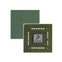
MPC8544VTALF Freescale Semiconductor, MPC8544VTALF Datasheet - Page 178

MPC8544VTALF
Manufacturer Part Number
MPC8544VTALF
Description
MPU POWERQUICC III 783-PBGA
Manufacturer
Freescale Semiconductor
Datasheets
1.MPC8544VTALF.pdf
(117 pages)
2.MPC8544VTALF.pdf
(2 pages)
3.MPC8544VTALF.pdf
(1340 pages)
Specifications of MPC8544VTALF
Processor Type
MPC85xx PowerQUICC III 32-Bit
Speed
667MHz
Voltage
1V
Mounting Type
Surface Mount
Package / Case
783-FCPBGA
Processor Series
MPC85xx
Core
e500
Data Bus Width
32 bit
Maximum Clock Frequency
667 MHz
Maximum Operating Temperature
+ 105 C
Mounting Style
SMD/SMT
Data Ram Size
32 KB
I/o Voltage
1.8 V, 3.3 V
Interface Type
I2C, HSSI, DUART
Minimum Operating Temperature
0 C
Lead Free Status / RoHS Status
Lead free / RoHS Compliant
Features
-
Lead Free Status / Rohs Status
Lead free / RoHS Compliant
Available stocks
Company
Part Number
Manufacturer
Quantity
Price
Company:
Part Number:
MPC8544VTALF
Manufacturer:
Freescale Semiconductor
Quantity:
10 000
Company:
Part Number:
MPC8544VTALFA
Manufacturer:
Freescale Semiconductor
Quantity:
10 000
- Current page: 178 of 1340
- Download datasheet (12Mb)
Reset, Clocking, and Initialization
4.4.3.14
The eTSEC3 protocol inputs, shown in
the eTSEC3 controller. Note that the value latched on these signals during POR is accessible through the
memory-mapped PORDEVSR (POR device status register) described in
Status Register (PORDEVSR).”
4.4.3.15
As shown in
clock--either a 100MHz or 125MHz LVDS differential clock. This one clock is applied to an internal PLL
whose output creates the clock used by all four SGMII SerDes lanes. The result is always a 1.25Gbaud
transmission/receive rate on each lane. Note that the value latched on this signal is accessible through the
memory-mapped SerDes Control and Status Register described in
Register 3
4-20
TSEC1_TXD[0:1]
Functional Signal
TSEC3_TXD[0:1]
Default (11)
Functional
Default (11)
Signal
(SRDS2CR3).”
Table
eTSEC3 Protocol
SGMII SerDes Reference Clock Configuration
MPC8544E PowerQUICC III Integrated Host Processor Family Reference Manual, Rev. 1
Reset Configuration
cfg_tsec1_prtcl[0:1]
Reset Configuration
cfg_tsec3_prtcl[0:1]
4-24, two options are available for the frequency of the input SGMII SerDes reference
Name
Name
Table 4-22. eTSEC1 Protocol Configuration
Table 4-23. eTSEC3 Protocol Configuration
(Binary)
Value
(Binary)
00
01
10
11
Value
00
01
10
11
Table
The eTSEC1 controller operates using 8-bit FIFO protocol.
The eTSEC1 controller operates using the MII protocol (or RMII if
configured in reduced mode as described in
width”).
The eTSEC1 controller operates using the GMII protocol (or RGMII if
configured in reduced mode as described in
width”).
The eTSEC1 controller operates using the TBI protocol (or RTBI if
configured in reduced mode as described in
width”) (default).
The eTSEC3 controller operates using 8-bit FIFO protocol.
The eTSEC3 controller operates using the MII protocol (or RMII if
configured in reduced mode as described in
Width”)
The eTSEC3 controller operates using the GMII protocol (or RGMII if
configured in reduced mode as described in
Width”).
The eTSEC3 controller operates using the TBI protocol (or RTBI if
configured in reduced mode as described in
Width”) (default).
4-23, select the protocol (FIFO, MII, GMII or TBI) used by
Section 19.4.1.26, “SerDes 2 Control
Meaning
Meaning
Section 19.4.1.4, “POR Device
Section 4.4.3.11, “eTSEC1
Section 4.4.3.11, “eTSEC1
Section 4.4.3.11, “eTSEC1
Section 4.4.3.12, “eTSEC3
Section 4.4.3.12, “eTSEC3
Section 4.4.3.12, “eTSEC3
Freescale Semiconductor
Related parts for MPC8544VTALF
Image
Part Number
Description
Manufacturer
Datasheet
Request
R
Part Number:
Description:
Manufacturer:
Freescale Semiconductor, Inc
Datasheet:
Part Number:
Description:
Manufacturer:
Freescale Semiconductor, Inc
Datasheet:
Part Number:
Description:
Manufacturer:
Freescale Semiconductor, Inc
Datasheet:
Part Number:
Description:
Manufacturer:
Freescale Semiconductor, Inc
Datasheet:
Part Number:
Description:
Manufacturer:
Freescale Semiconductor, Inc
Datasheet:
Part Number:
Description:
Manufacturer:
Freescale Semiconductor, Inc
Datasheet:
Part Number:
Description:
Manufacturer:
Freescale Semiconductor, Inc
Datasheet:
Part Number:
Description:
Manufacturer:
Freescale Semiconductor, Inc
Datasheet:
Part Number:
Description:
Manufacturer:
Freescale Semiconductor, Inc
Datasheet:
Part Number:
Description:
Manufacturer:
Freescale Semiconductor, Inc
Datasheet:
Part Number:
Description:
Manufacturer:
Freescale Semiconductor, Inc
Datasheet:
Part Number:
Description:
Manufacturer:
Freescale Semiconductor, Inc
Datasheet:
Part Number:
Description:
Manufacturer:
Freescale Semiconductor, Inc
Datasheet:
Part Number:
Description:
Manufacturer:
Freescale Semiconductor, Inc
Datasheet:
Part Number:
Description:
Manufacturer:
Freescale Semiconductor, Inc
Datasheet:


