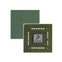
MPC8544VTALF Freescale Semiconductor, MPC8544VTALF Datasheet - Page 288

MPC8544VTALF
Manufacturer Part Number
MPC8544VTALF
Description
MPU POWERQUICC III 783-PBGA
Manufacturer
Freescale Semiconductor
Datasheets
1.MPC8544VTALF.pdf
(117 pages)
2.MPC8544VTALF.pdf
(2 pages)
3.MPC8544VTALF.pdf
(1340 pages)
Specifications of MPC8544VTALF
Processor Type
MPC85xx PowerQUICC III 32-Bit
Speed
667MHz
Voltage
1V
Mounting Type
Surface Mount
Package / Case
783-FCPBGA
Processor Series
MPC85xx
Core
e500
Data Bus Width
32 bit
Maximum Clock Frequency
667 MHz
Maximum Operating Temperature
+ 105 C
Mounting Style
SMD/SMT
Data Ram Size
32 KB
I/o Voltage
1.8 V, 3.3 V
Interface Type
I2C, HSSI, DUART
Minimum Operating Temperature
0 C
Lead Free Status / RoHS Status
Lead free / RoHS Compliant
Features
-
Lead Free Status / Rohs Status
Lead free / RoHS Compliant
Available stocks
Company
Part Number
Manufacturer
Quantity
Price
Company:
Part Number:
MPC8544VTALF
Manufacturer:
Freescale Semiconductor
Quantity:
10 000
Company:
Part Number:
MPC8544VTALFA
Manufacturer:
Freescale Semiconductor
Quantity:
10 000
- Current page: 288 of 1340
- Download datasheet (12Mb)
L2 Look-Aside Cache/SRAM
7.3.1.4.1
The L2 cache includes support for injecting errors into the L2 data, data ECC, or tag. This may be used to
test error recovery software by deterministically creating error scenarios.
The preferred method for error injection is to set all data pages to cache-inhibited (MMU TLB entry I = 1)
except a scratch page, set L2CTL[L2DO] to prevent allocation of instruction accesses, and invalidate the
L2 by setting L2CTL[L2I] = 1. The following code sequence triggers an error, then detects it (A is an
address in the scratch page):
Data or tag errors are injected into the line, according to the error injection settings in L2ERRINJHI,
L2ERRINJLO, and L2ERRINJCTL, at allocation. The final load detects and reports the error (if enabled)
and allows software to examine the offending data, address, and attributes.
Note that error injection enable bits in L2ERRINJCTL must be cleared by software and the L2 must be
invalidated (by setting L2CTL[L2I]) before resuming L2 normal operation.
error injection mask high register (L2ERRINJHI).
Table 7-10
Figure 7-14
7-18
Offset 0x2_0E00
Offset 0x2_0E04
Reset
0–31
Reset
Bits
dcbz A
dcbtls_L2 A
lwz A
W
W
R
R
0
0
EIMASKHI Error injection mask/high word. A set bit corresponding to a data path bit causes that bit on the data path
Name
describes L2ERRINJHI[EIMASKHI].
shows the L2 error injection mask low register (L2ERRINJLO).
MPC8544E PowerQUICC III Integrated Host Processor Family Reference Manual, Rev. 1
Error Injection Registers
to be inverted on cache/SRAM writes if L2ERRINJCTL[DERRIEN] = 1.
Figure 7-14. L2 Error Injection Mask Low Register (L2ERRINJLO)
Figure 7-13. L2 Error Injection Mask High Register (L2ERRINJHI)
| allocates the line in the L1 in the modified state
| forces the line from the L1 and allocates the line in the L2
Table 7-10. L2ERRINJHI Field Description
EIMASKLO
EIMASKHI
All zeros
All zeros
Description
Figure 7-13
Freescale Semiconductor
Access: Read/Write
Access: Read/Write
shows the L2
31
31
Related parts for MPC8544VTALF
Image
Part Number
Description
Manufacturer
Datasheet
Request
R
Part Number:
Description:
Manufacturer:
Freescale Semiconductor, Inc
Datasheet:
Part Number:
Description:
Manufacturer:
Freescale Semiconductor, Inc
Datasheet:
Part Number:
Description:
Manufacturer:
Freescale Semiconductor, Inc
Datasheet:
Part Number:
Description:
Manufacturer:
Freescale Semiconductor, Inc
Datasheet:
Part Number:
Description:
Manufacturer:
Freescale Semiconductor, Inc
Datasheet:
Part Number:
Description:
Manufacturer:
Freescale Semiconductor, Inc
Datasheet:
Part Number:
Description:
Manufacturer:
Freescale Semiconductor, Inc
Datasheet:
Part Number:
Description:
Manufacturer:
Freescale Semiconductor, Inc
Datasheet:
Part Number:
Description:
Manufacturer:
Freescale Semiconductor, Inc
Datasheet:
Part Number:
Description:
Manufacturer:
Freescale Semiconductor, Inc
Datasheet:
Part Number:
Description:
Manufacturer:
Freescale Semiconductor, Inc
Datasheet:
Part Number:
Description:
Manufacturer:
Freescale Semiconductor, Inc
Datasheet:
Part Number:
Description:
Manufacturer:
Freescale Semiconductor, Inc
Datasheet:
Part Number:
Description:
Manufacturer:
Freescale Semiconductor, Inc
Datasheet:
Part Number:
Description:
Manufacturer:
Freescale Semiconductor, Inc
Datasheet:


