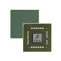
MPC8544VTALF Freescale Semiconductor, MPC8544VTALF Datasheet - Page 145

MPC8544VTALF
Manufacturer Part Number
MPC8544VTALF
Description
MPU POWERQUICC III 783-PBGA
Manufacturer
Freescale Semiconductor
Datasheets
1.MPC8544VTALF.pdf
(117 pages)
2.MPC8544VTALF.pdf
(2 pages)
3.MPC8544VTALF.pdf
(1340 pages)
Specifications of MPC8544VTALF
Processor Type
MPC85xx PowerQUICC III 32-Bit
Speed
667MHz
Voltage
1V
Mounting Type
Surface Mount
Package / Case
783-FCPBGA
Processor Series
MPC85xx
Core
e500
Data Bus Width
32 bit
Maximum Clock Frequency
667 MHz
Maximum Operating Temperature
+ 105 C
Mounting Style
SMD/SMT
Data Ram Size
32 KB
I/o Voltage
1.8 V, 3.3 V
Interface Type
I2C, HSSI, DUART
Minimum Operating Temperature
0 C
Lead Free Status / RoHS Status
Lead free / RoHS Compliant
Features
-
Lead Free Status / Rohs Status
Lead free / RoHS Compliant
Available stocks
Company
Part Number
Manufacturer
Quantity
Price
Company:
Part Number:
MPC8544VTALF
Manufacturer:
Freescale Semiconductor
Quantity:
10 000
Company:
Part Number:
MPC8544VTALFA
Manufacturer:
Freescale Semiconductor
Quantity:
10 000
- Current page: 145 of 1340
- Download datasheet (12Mb)
Note that individual chapters of this document provide details for each signal, describing each signal’s
behavior when the signal is asserted or negated and when the signal is an input or an output.
The following tables provide summaries of signal functions.
and
number of signals, and whether the signal is an input, output, or bidirectional. The direction of the
multiplexed signals applies for the primary signal function listed in the left-most column of the table for
that row (and does not apply for the state of the reset configuration signals). Finally, the tables provide a
pointer to the table where the signal function is described.
Freescale Semiconductor
PCI_C/BE[3:0]
PCI_DEVSEL
PCI_AD[31:0]
PCI_FRAME
PCI_IDSEL
MDQ[0:63]
MECC[0:7]
MDQS[0:7]
MDQS[0:8]
MCKE[0:3]
MODT[0:3]
PCI_TRDY
PCI_STOP
MCK[0:5],
MDIC[0:1]
PCI_IRDY
MDM[0:7]
Table 3-2
MBA[2:0]
MCS[0:3]
MCK[0:5]
PCI_PAR
MA[15:0]
MDQS8
MDM8
MRAS
MCAS
Name
MWE
lists signals alphabetically. These tables detail the signal name, interface, alternate functions,
MPC8544E PowerQUICC III Integrated Host Processor Family Reference Manual, Rev. 1
DDR data
DDR error correcting code
DDR data mask
DDR ECC data mask
DDR data strobe
DDR ECC data strobe
DDR ECC data strobe
(complement)
DDR bank select
DDR address
DDR write enable
DDR row address strobe
DDR column address strobe
DDR chip select (2/DIMM)
DDR clock enable
DDR differential clocks (3
pairs/DIMM)
DRAM On-Die Termination
Driver impedence calibration
PCI address/data
PCI command/byte enable
PCI parity
PCI frame
PCI target ready
PCI initiator ready
PCI stop
PCI device select
PCI initial device select
Table 3-1. MPC8544E Signal Reference by Functional Block
Description
DDR memory
DDR memory
DDR memory
DDR memory
DDR memory
DDR memory
DDR memory
DDR memory
DDR memory
DDR memory
DDR memory
DDR memory
DDR memory
DDR memory
DDR memory
DDR memory
DDR memory
Functional
Debug/
Block
PCI
PCI
PCI
PCI
PCI
PCI
PCI
PCI
PCI
Alternate Function(s)
Table 3-1
—
—
—
—
—
—
—
—
—
—
—
—
—
—
—
—
—
—
—
—
—
—
—
—
—
—
lists signals grouped by function,
Signals
No. of
64
16
12
32
8
8
1
8
1
9
3
1
1
1
4
4
4
2
4
1
1
1
1
1
1
1
I/O
I/O
I/O
I/O
I/O
I/O
I/O
I/O
I/O
I/O
I/O
I/O
I/O
I/O
I/O
O
O
O
O
O
O
O
O
O
O
O
I
Signal Descriptions
17-2/17-6
17-2/17-6
17-2/17-6
17-2/17-6
17-2/17-6
17-2/17-6
17-2/17-6
17-2/17-6
17-2/17-6
9-3/9-5
9-3/9-5
9-3/9-5
9-3/9-5
9-3/9-5
9-3/9-5
9-3/9-5
9-3/9-5
9-3/9-5
9-3/9-5
9-3/9-5
9-3/9-5
9-3/9-5
9-3/9-5
9-3/9-5
Table/
Page
3-5
Related parts for MPC8544VTALF
Image
Part Number
Description
Manufacturer
Datasheet
Request
R
Part Number:
Description:
Manufacturer:
Freescale Semiconductor, Inc
Datasheet:
Part Number:
Description:
Manufacturer:
Freescale Semiconductor, Inc
Datasheet:
Part Number:
Description:
Manufacturer:
Freescale Semiconductor, Inc
Datasheet:
Part Number:
Description:
Manufacturer:
Freescale Semiconductor, Inc
Datasheet:
Part Number:
Description:
Manufacturer:
Freescale Semiconductor, Inc
Datasheet:
Part Number:
Description:
Manufacturer:
Freescale Semiconductor, Inc
Datasheet:
Part Number:
Description:
Manufacturer:
Freescale Semiconductor, Inc
Datasheet:
Part Number:
Description:
Manufacturer:
Freescale Semiconductor, Inc
Datasheet:
Part Number:
Description:
Manufacturer:
Freescale Semiconductor, Inc
Datasheet:
Part Number:
Description:
Manufacturer:
Freescale Semiconductor, Inc
Datasheet:
Part Number:
Description:
Manufacturer:
Freescale Semiconductor, Inc
Datasheet:
Part Number:
Description:
Manufacturer:
Freescale Semiconductor, Inc
Datasheet:
Part Number:
Description:
Manufacturer:
Freescale Semiconductor, Inc
Datasheet:
Part Number:
Description:
Manufacturer:
Freescale Semiconductor, Inc
Datasheet:
Part Number:
Description:
Manufacturer:
Freescale Semiconductor, Inc
Datasheet:


