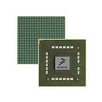
MPC8544VTALF Freescale Semiconductor, MPC8544VTALF Datasheet - Page 303

MPC8544VTALF
Manufacturer Part Number
MPC8544VTALF
Description
MPU POWERQUICC III 783-PBGA
Manufacturer
Freescale Semiconductor
Datasheets
1.MPC8544VTALF.pdf
(117 pages)
2.MPC8544VTALF.pdf
(2 pages)
3.MPC8544VTALF.pdf
(1340 pages)
Specifications of MPC8544VTALF
Processor Type
MPC85xx PowerQUICC III 32-Bit
Speed
667MHz
Voltage
1V
Mounting Type
Surface Mount
Package / Case
783-FCPBGA
Processor Series
MPC85xx
Core
e500
Data Bus Width
32 bit
Maximum Clock Frequency
667 MHz
Maximum Operating Temperature
+ 105 C
Mounting Style
SMD/SMT
Data Ram Size
32 KB
I/o Voltage
1.8 V, 3.3 V
Interface Type
I2C, HSSI, DUART
Minimum Operating Temperature
0 C
Lead Free Status / RoHS Status
Lead free / RoHS Compliant
Features
-
Lead Free Status / Rohs Status
Lead free / RoHS Compliant
Available stocks
Company
Part Number
Manufacturer
Quantity
Price
Company:
Part Number:
MPC8544VTALF
Manufacturer:
Freescale Semiconductor
Quantity:
10 000
Company:
Part Number:
MPC8544VTALFA
Manufacturer:
Freescale Semiconductor
Quantity:
10 000
- Current page: 303 of 1340
- Download datasheet (12Mb)
An effective value of each PLRU bit is calculated as follows:
These effective PLRU bits are used to select a victim, as indicated in
7.9
This section describes the behavior of the L1 and L2 cache in response to various operations and in various
configurations.
7.9.1
7.9.1.1
After power-on reset the valid bits in the L2 cache status array are in random states. Therefore, it is
necessary to perform a flash invalidate before using the array as an L2 cache. This is done by writing a one
to the L2I field of the L2 control register (L2CTL). This can be done before or simultaneously with the
write that enables the L2 cache. That is, the L2E and L2I bits of L2CTL can be set simultaneously. The
L2I bit clears automatically, so no further writes are necessary.
7.9.1.2
After power-on reset the contents of the data and ECC arrays are random, so all SRAM data must be
initialized before it is read. If the cache is initialized by the processor or any other device that uses
sub-cache-line transactions, ECC error checking should be disabled during the initialization process to
avoid false ECC errors generated during the read-modify-write process used for sub-cache-line writes to
the SRAM array. This is done by setting the multi- and single-bit ECC error disable bits of the L2 error
Freescale Semiconductor
P0_eff = f(P0,L0,L1,L2,L3,L4,L5,L6,L7) = (L0 & L1 & L2 & L3) | (P0 & ~(L4 & L5 & L6 & L7))
P1_eff = f(P1,L0,L1,L2,L3) = (L0 & L1) | (P1 & ~(L2 & L3))
P2_eff = f(P2,L4,L5,L6,L7) = (L4 & L5) | (P2 & ~(L6 & L7))
P3_eff = f(P3,L0,L1) = L0 | (P3 & ~L1)
P4_eff = f(P4,L2,L3) = L2 | (P4 & ~L3)
P5_eff = f(P5,L4,L5) = L4 | (P5 & ~L5)
P6_eff = f(P6,L6,L7) = L6 | (P6 & ~L7)
L2 Cache Operation
Initialization
MPC8544E PowerQUICC III Integrated Host Processor Family Reference Manual, Rev. 1
L2 Cache Initialization
Memory-Mapped SRAM Initialization
Way Selected
Table 7-25. PLRU-Based Victim Selection Mechanism
W0
W1
W2
W3
W4
W5
W6
W7
Effective PLRU
State (Binary)
00x0xxx
00x1xxx
01xx0xx
01xx1xx
1x0xx0x
1x0xx1x
1x1xxx0
1x1xxx1
(using effective PLRU bits)
Reduced Logic Equation
~P0 & ~P1 & ~P3
~P0 & ~P1 & P3
~P0 & P1 & ~P4
P0 & ~P2 & ~P5
P0 & ~P2 & P5
P0 & P2 & ~P6
~P0 & P1 & P4
P0 & P2 & P6
Table
7-25.
L2 Look-Aside Cache/SRAM
7-33
Related parts for MPC8544VTALF
Image
Part Number
Description
Manufacturer
Datasheet
Request
R
Part Number:
Description:
Manufacturer:
Freescale Semiconductor, Inc
Datasheet:
Part Number:
Description:
Manufacturer:
Freescale Semiconductor, Inc
Datasheet:
Part Number:
Description:
Manufacturer:
Freescale Semiconductor, Inc
Datasheet:
Part Number:
Description:
Manufacturer:
Freescale Semiconductor, Inc
Datasheet:
Part Number:
Description:
Manufacturer:
Freescale Semiconductor, Inc
Datasheet:
Part Number:
Description:
Manufacturer:
Freescale Semiconductor, Inc
Datasheet:
Part Number:
Description:
Manufacturer:
Freescale Semiconductor, Inc
Datasheet:
Part Number:
Description:
Manufacturer:
Freescale Semiconductor, Inc
Datasheet:
Part Number:
Description:
Manufacturer:
Freescale Semiconductor, Inc
Datasheet:
Part Number:
Description:
Manufacturer:
Freescale Semiconductor, Inc
Datasheet:
Part Number:
Description:
Manufacturer:
Freescale Semiconductor, Inc
Datasheet:
Part Number:
Description:
Manufacturer:
Freescale Semiconductor, Inc
Datasheet:
Part Number:
Description:
Manufacturer:
Freescale Semiconductor, Inc
Datasheet:
Part Number:
Description:
Manufacturer:
Freescale Semiconductor, Inc
Datasheet:
Part Number:
Description:
Manufacturer:
Freescale Semiconductor, Inc
Datasheet:


