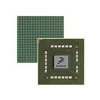
MPC8544VTALF Freescale Semiconductor, MPC8544VTALF Datasheet - Page 289

MPC8544VTALF
Manufacturer Part Number
MPC8544VTALF
Description
MPU POWERQUICC III 783-PBGA
Manufacturer
Freescale Semiconductor
Datasheets
1.MPC8544VTALF.pdf
(117 pages)
2.MPC8544VTALF.pdf
(2 pages)
3.MPC8544VTALF.pdf
(1340 pages)
Specifications of MPC8544VTALF
Processor Type
MPC85xx PowerQUICC III 32-Bit
Speed
667MHz
Voltage
1V
Mounting Type
Surface Mount
Package / Case
783-FCPBGA
Processor Series
MPC85xx
Core
e500
Data Bus Width
32 bit
Maximum Clock Frequency
667 MHz
Maximum Operating Temperature
+ 105 C
Mounting Style
SMD/SMT
Data Ram Size
32 KB
I/o Voltage
1.8 V, 3.3 V
Interface Type
I2C, HSSI, DUART
Minimum Operating Temperature
0 C
Lead Free Status / RoHS Status
Lead free / RoHS Compliant
Features
-
Lead Free Status / Rohs Status
Lead free / RoHS Compliant
Available stocks
Company
Part Number
Manufacturer
Quantity
Price
Company:
Part Number:
MPC8544VTALF
Manufacturer:
Freescale Semiconductor
Quantity:
10 000
Company:
Part Number:
MPC8544VTALFA
Manufacturer:
Freescale Semiconductor
Quantity:
10 000
- Current page: 289 of 1340
- Download datasheet (12Mb)
Table 7-11
Figure 7-15
Table 7-12
Freescale Semiconductor
Offset 0x2_0E08
Reset
16–21
24–31
0–31
0–14
Bits
Bits
15
22
23
W
R
0
EIMASKLO Error injection mask/low word. A set bit corresponding to a data path bit causes that bit on the data path
ECCERRIM Error injection mask for the ECC bits. A set bit corresponding to an ECC bit causes that bit to be
DERRIEN
TERRIEN
ECCMB
describes L2ERRINJLO[EIMASKLO].
Name
describes L2ERRINJCTL fields.
Name
shows the L2 error injection mask control register (L2ERRINJCTL).
—
—
MPC8544E PowerQUICC III Integrated Host Processor Family Reference Manual, Rev. 1
Figure 7-15. L2 Error Injection Mask Control Register (L2ERRINJCTL)
to be inverted on SRAM writes if L2ERRINJCTL[DERRIEN] = 1.
Reserved
0 No tag errors are injected.
1 All subsequent entries written to the L2 tag array have the parity bit inverted.
Reserved
0 ECC byte mirroring is disabled
1 The most significant data path byte is mirrored onto the ECC byte if DERRIEN = 1.
0 No data errors are injected.
1 Subsequent entries written to the L2 data array have data or ECC bits inverted as specified in the
Note: if both ECC mirror byte and data error injection are enabled, ECC mask error injection is
performed on the mirrored ECC.
inverted on SRAM writes if DERRIEN = 1.
L2 tag array error injection enable
ECC mirror byte enable.
L2 data array error injection enable:
—
data and ECC error injection masks and/or data path byte mirrored onto ECC as specified by ECC
mirror byte enable.
Table 7-12. L2ERRINJCTL Field Descriptions
Table 7-11. L2ERRINJLO Field Description
14
TERRIEN
15
16
All zeros
—
Description
Description
21
ECCMB
22
DERRIEN
23
L2 Look-Aside Cache/SRAM
24
Access: Read/Write
ECCERRIM
7-19
31
Related parts for MPC8544VTALF
Image
Part Number
Description
Manufacturer
Datasheet
Request
R
Part Number:
Description:
Manufacturer:
Freescale Semiconductor, Inc
Datasheet:
Part Number:
Description:
Manufacturer:
Freescale Semiconductor, Inc
Datasheet:
Part Number:
Description:
Manufacturer:
Freescale Semiconductor, Inc
Datasheet:
Part Number:
Description:
Manufacturer:
Freescale Semiconductor, Inc
Datasheet:
Part Number:
Description:
Manufacturer:
Freescale Semiconductor, Inc
Datasheet:
Part Number:
Description:
Manufacturer:
Freescale Semiconductor, Inc
Datasheet:
Part Number:
Description:
Manufacturer:
Freescale Semiconductor, Inc
Datasheet:
Part Number:
Description:
Manufacturer:
Freescale Semiconductor, Inc
Datasheet:
Part Number:
Description:
Manufacturer:
Freescale Semiconductor, Inc
Datasheet:
Part Number:
Description:
Manufacturer:
Freescale Semiconductor, Inc
Datasheet:
Part Number:
Description:
Manufacturer:
Freescale Semiconductor, Inc
Datasheet:
Part Number:
Description:
Manufacturer:
Freescale Semiconductor, Inc
Datasheet:
Part Number:
Description:
Manufacturer:
Freescale Semiconductor, Inc
Datasheet:
Part Number:
Description:
Manufacturer:
Freescale Semiconductor, Inc
Datasheet:
Part Number:
Description:
Manufacturer:
Freescale Semiconductor, Inc
Datasheet:


