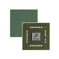
MPC8544VTALF Freescale Semiconductor, MPC8544VTALF Datasheet - Page 283

MPC8544VTALF
Manufacturer Part Number
MPC8544VTALF
Description
MPU POWERQUICC III 783-PBGA
Manufacturer
Freescale Semiconductor
Datasheets
1.MPC8544VTALF.pdf
(117 pages)
2.MPC8544VTALF.pdf
(2 pages)
3.MPC8544VTALF.pdf
(1340 pages)
Specifications of MPC8544VTALF
Processor Type
MPC85xx PowerQUICC III 32-Bit
Speed
667MHz
Voltage
1V
Mounting Type
Surface Mount
Package / Case
783-FCPBGA
Processor Series
MPC85xx
Core
e500
Data Bus Width
32 bit
Maximum Clock Frequency
667 MHz
Maximum Operating Temperature
+ 105 C
Mounting Style
SMD/SMT
Data Ram Size
32 KB
I/o Voltage
1.8 V, 3.3 V
Interface Type
I2C, HSSI, DUART
Minimum Operating Temperature
0 C
Lead Free Status / RoHS Status
Lead free / RoHS Compliant
Features
-
Lead Free Status / Rohs Status
Lead free / RoHS Compliant
Available stocks
Company
Part Number
Manufacturer
Quantity
Price
Company:
Part Number:
MPC8544VTALF
Manufacturer:
Freescale Semiconductor
Quantity:
10 000
Company:
Part Number:
MPC8544VTALFA
Manufacturer:
Freescale Semiconductor
Quantity:
10 000
- Current page: 283 of 1340
- Download datasheet (12Mb)
7.3.1.2
The device supports allocating and locking L2 cache lines from external agents such as PCI. This
functionality is called stashing. Four sets of registers are provided to support this feature; each set has three
registers that specify a programmed memory range that can be locked with a snoop write transaction. All
three registers in a set must be configured in order to use an external write address.
These registers are the L2 cache external write address registers 0–3 (L2CEWARn), the L2 cache external
write address registers extended address 0–3 (L2CEWAREAn), and the L2 cache external write control
registers 0–3 (L2CEWCRn). L2CEWARn contain the lower 24 bits of the external write base address and
L2CEWAREAn contain the upper 4 bits. The base address specified in the address registers must be
naturally aligned to the window size in the corresponding control register.
Further details on the locations and fields of these registers are given in the following sections.
7.3.1.2.1
The L2CEWARn registers contain the lower 24 bits of the 28-bit L2 cache external write base address.
Each of these registers has identical fields, as shown in
Freescale Semiconductor
30–31
Bits
Offset 0x2_0010
29
Reset
W
R
L2STASHCTL
0x2_0020
0x2_0030
0x2_0040
0
Name
—
MPC8544E PowerQUICC III Integrated Host Processor Family Reference Manual, Rev. 1
L2 Cache External Write Registers
L2 Cache External Write Address Registers 0–3 (L2CEWAR n )
Figure 7-8. Cache External Write Address Registers (L2CEWAR n )
Reserved
L2 stash configuration. This field reserves regions of the cache for stash-only operation. That is, blocks
of each cache set are reserved so that they can only be allocated for stash data. If such a region is
created, processor reads and writes will not be allocated into this region; it can only be populated by
stash writes. Similarly, stash writes will only be allocated into this region. This prevents processor and
stashed I/O data from polluting one another.
00 No stash-only region. Stashed writes will be allocated across the entire cache and can evict
01 One half of the array is a stash-only cache (way4, way5, way6 & way7 of each set)
10 One quarter of the array is a stash-only cache (way6 & way7 of each set)
11 One eighth of the array is a stash-only cache (way7 of each set)
Like L2SRAM configuration, stash-only regions subtract from the amount of the on-chip memory that
is available to the processor as cache. If the L2SRAM configuration uses the entire on-chip memory
array as SRAM, then no stash-only region can be created.
To change these bits, the L2 must be disabled (L2CTL[L2E] = 0). This field has no effect if the
L2STASHDIS bit is set.
processor data and can be evicted by processor data.
Table 7-4. L2CTL Field Descriptions (continued)
ADDR
All zeros
Figure
Description
7-8.
23 24
L2 Look-Aside Cache/SRAM
Access: Read/Write
—
7-13
31
Related parts for MPC8544VTALF
Image
Part Number
Description
Manufacturer
Datasheet
Request
R
Part Number:
Description:
Manufacturer:
Freescale Semiconductor, Inc
Datasheet:
Part Number:
Description:
Manufacturer:
Freescale Semiconductor, Inc
Datasheet:
Part Number:
Description:
Manufacturer:
Freescale Semiconductor, Inc
Datasheet:
Part Number:
Description:
Manufacturer:
Freescale Semiconductor, Inc
Datasheet:
Part Number:
Description:
Manufacturer:
Freescale Semiconductor, Inc
Datasheet:
Part Number:
Description:
Manufacturer:
Freescale Semiconductor, Inc
Datasheet:
Part Number:
Description:
Manufacturer:
Freescale Semiconductor, Inc
Datasheet:
Part Number:
Description:
Manufacturer:
Freescale Semiconductor, Inc
Datasheet:
Part Number:
Description:
Manufacturer:
Freescale Semiconductor, Inc
Datasheet:
Part Number:
Description:
Manufacturer:
Freescale Semiconductor, Inc
Datasheet:
Part Number:
Description:
Manufacturer:
Freescale Semiconductor, Inc
Datasheet:
Part Number:
Description:
Manufacturer:
Freescale Semiconductor, Inc
Datasheet:
Part Number:
Description:
Manufacturer:
Freescale Semiconductor, Inc
Datasheet:
Part Number:
Description:
Manufacturer:
Freescale Semiconductor, Inc
Datasheet:
Part Number:
Description:
Manufacturer:
Freescale Semiconductor, Inc
Datasheet:


