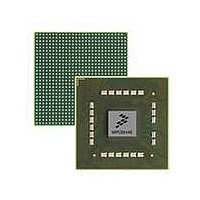
MPC8544VTALF Freescale Semiconductor, MPC8544VTALF Datasheet - Page 1045

MPC8544VTALF
Manufacturer Part Number
MPC8544VTALF
Description
MPU POWERQUICC III 783-PBGA
Manufacturer
Freescale Semiconductor
Datasheets
1.MPC8544VTALF.pdf
(117 pages)
2.MPC8544VTALF.pdf
(2 pages)
3.MPC8544VTALF.pdf
(1340 pages)
Specifications of MPC8544VTALF
Processor Type
MPC85xx PowerQUICC III 32-Bit
Speed
667MHz
Voltage
1V
Mounting Type
Surface Mount
Package / Case
783-FCPBGA
Processor Series
MPC85xx
Core
e500
Data Bus Width
32 bit
Maximum Clock Frequency
667 MHz
Maximum Operating Temperature
+ 105 C
Mounting Style
SMD/SMT
Data Ram Size
32 KB
I/o Voltage
1.8 V, 3.3 V
Interface Type
I2C, HSSI, DUART
Minimum Operating Temperature
0 C
Lead Free Status / RoHS Status
Lead free / RoHS Compliant
Features
-
Lead Free Status / Rohs Status
Lead free / RoHS Compliant
Available stocks
Company
Part Number
Manufacturer
Quantity
Price
Company:
Part Number:
MPC8544VTALF
Manufacturer:
Freescale Semiconductor
Quantity:
10 000
Company:
Part Number:
MPC8544VTALFA
Manufacturer:
Freescale Semiconductor
Quantity:
10 000
- Current page: 1045 of 1340
- Download datasheet (12Mb)
17.4.2.11.3 Agent Accessing the PCI Configuration Space
When this device is configured as an agent device, it responds to a remote host-generated PCI
configuration cycle. This is indicated by decoding the configuration command along with PCI's IDSEL
being asserted. When the PCI controller detects an access to PCI CFG_DATA, it checks the enable flag
and the device number in the PCI CFG_ADDR register. If the enable bit is set, and the device number is
not 0b1_1111, the PCI controller performs a configuration cycle translation function and runs a
configuration-read or configuration-write transaction on the PCI bus. The device number 0b1_1111 is used
for performing interrupt-acknowledge and special-cycle transactions. See
Transactions,”
0x00), the PCI controller performs a type 0 configuration cycle translation. If the bus number indicates a
remote PCI bus (that is, nonlocal), the PCI controller performs a type 1 configuration cycle translation.
Note that in the following examples, the data in the configuration register is shown in little-endian order.
This is because all the PCI registers are intrinsically little-endian. External PCI masters that use the local
address map to access configuration space do not need to reverse bytes since byte lane redirection from
the little-endian PCI bus is performed internally.
Example: Configuration sequence, 4-byte data write to PCI register at address offset 0x14 of Device 1 on
PCI bus 0.
Initial values:
Code sequence:
Results:
Example: Configuration sequence, 2-byte data write to PCI register at address offset 0x1C of Device 1 on
PCI bus 0.
Initial values:
Code sequence:
Results:
Freescale Semiconductor
r0 contains 0x8000_0814
r1 contains CCSRBAR + BlockBase + 0x000 (Address of PCI CFG_ADDR register)
r2 contains CCSRBAR + BlockBase + 0x004 (Address of PCI CFG_DATA register)
r3 contains 0x1122_3344
Register at 0x14 contains 0xFFFF_FFFF (0x17 to 0x14)
stw r0, 0 (r1) // Update PCI CFG_ADDR register to point to
stwbrx r3, 0 (r2)
Address CCSRBAR + BlockBase + 0x000 contains 0x8000_0814
Register at 0x14 contains 0x1122_3344 (0x17 to 0x14)
r0 contains 0x8000_081C
r1 contains CCSRBAR + BlockBase + 0x000
r2 contains CCSRBAR + BlockBase + 0x004
r3 contains 0xDDCC_BBAA
Register at 0x1C contains 0xFFFF_FFFF (0x1F to 0x1C)
stw r0, 0 (r1)
sthbrx r3, 0 (r2)
Address CCSRBAR + BlockBase + 0x000 contains 0x8000_081C
Register at 0x1C contains 0xFFFF_BBAA (0x1F to 0x1C)
MPC8544E PowerQUICC III Integrated Host Processor Family Reference Manual, Rev. 1
for more information. If the bus number corresponds to the local PCI bus (bus number =
//register offset 0x14 of device 1.
Section 17.4.2.12, “Other Bus
PCI Bus Interface
17-61
Related parts for MPC8544VTALF
Image
Part Number
Description
Manufacturer
Datasheet
Request
R
Part Number:
Description:
Manufacturer:
Freescale Semiconductor, Inc
Datasheet:
Part Number:
Description:
Manufacturer:
Freescale Semiconductor, Inc
Datasheet:
Part Number:
Description:
Manufacturer:
Freescale Semiconductor, Inc
Datasheet:
Part Number:
Description:
Manufacturer:
Freescale Semiconductor, Inc
Datasheet:
Part Number:
Description:
Manufacturer:
Freescale Semiconductor, Inc
Datasheet:
Part Number:
Description:
Manufacturer:
Freescale Semiconductor, Inc
Datasheet:
Part Number:
Description:
Manufacturer:
Freescale Semiconductor, Inc
Datasheet:
Part Number:
Description:
Manufacturer:
Freescale Semiconductor, Inc
Datasheet:
Part Number:
Description:
Manufacturer:
Freescale Semiconductor, Inc
Datasheet:
Part Number:
Description:
Manufacturer:
Freescale Semiconductor, Inc
Datasheet:
Part Number:
Description:
Manufacturer:
Freescale Semiconductor, Inc
Datasheet:
Part Number:
Description:
Manufacturer:
Freescale Semiconductor, Inc
Datasheet:
Part Number:
Description:
Manufacturer:
Freescale Semiconductor, Inc
Datasheet:
Part Number:
Description:
Manufacturer:
Freescale Semiconductor, Inc
Datasheet:
Part Number:
Description:
Manufacturer:
Freescale Semiconductor, Inc
Datasheet:


