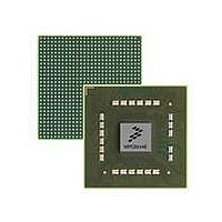
MPC8544VTALF Freescale Semiconductor, MPC8544VTALF Datasheet - Page 746

MPC8544VTALF
Manufacturer Part Number
MPC8544VTALF
Description
MPU POWERQUICC III 783-PBGA
Manufacturer
Freescale Semiconductor
Datasheets
1.MPC8544VTALF.pdf
(117 pages)
2.MPC8544VTALF.pdf
(2 pages)
3.MPC8544VTALF.pdf
(1340 pages)
Specifications of MPC8544VTALF
Processor Type
MPC85xx PowerQUICC III 32-Bit
Speed
667MHz
Voltage
1V
Mounting Type
Surface Mount
Package / Case
783-FCPBGA
Processor Series
MPC85xx
Core
e500
Data Bus Width
32 bit
Maximum Clock Frequency
667 MHz
Maximum Operating Temperature
+ 105 C
Mounting Style
SMD/SMT
Data Ram Size
32 KB
I/o Voltage
1.8 V, 3.3 V
Interface Type
I2C, HSSI, DUART
Minimum Operating Temperature
0 C
Lead Free Status / RoHS Status
Lead free / RoHS Compliant
Features
-
Lead Free Status / Rohs Status
Lead free / RoHS Compliant
Available stocks
Company
Part Number
Manufacturer
Quantity
Price
Company:
Part Number:
MPC8544VTALF
Manufacturer:
Freescale Semiconductor
Quantity:
10 000
Company:
Part Number:
MPC8544VTALFA
Manufacturer:
Freescale Semiconductor
Quantity:
10 000
- Current page: 746 of 1340
- Download datasheet (12Mb)
Enhanced Three-Speed Ethernet Controllers
15.5.2
Table 15-4
offsets to the memory map table are defined for both eTSECs. That is, eTSEC1 starts at 0x2_4000 address
offset and eTSEC3 starts at 0x2_5000 address offset. The registers for eTSEC1 are listed in
but the registers for the other eTSEC are not. Note that the registers are the same for eTSEC3 except that
the offset changes as previously explained and as noted at the end of
In this table and in the register figures and field descriptions, the following access definitions apply:
15-14
0x2_4008–
0x2_4034–
0x2_400C
0x2_401C Reserved
0x2_402C DMACTRL—DMA control register
0x2_410C Reserved
0x2_4000 TSEC_ID*—Controller ID register
0x2_4004 TSEC_ID2*—Controller ID register
0x2_4010 IEVENT—Interrupt event register
0x2_4014 IMASK—Interrupt mask register
0x2_4018 EDIS—Error disabled register
0x2_4020 ECNTRL—Ethernet control register
0x2_4024 Reserved
0x2_4028 PTV—Pause time value register
0x2_4030 TBIPA—TBI PHY address register
0x2_4054
0x2_4100 TCTRL—Transmit control register
0x2_4104 TSTAT—Transmit status register
0x2_4108 DFVLAN*—Default VLAN control word
eTSEC1
Offset
•
•
•
•
•
Reserved fields are always ignored for the purposes of determining access type.
R/W, R, and W (read/write, read only, and write only) indicate that all the non-reserved fields in a
register have the same access type.
w1c indicates that all of the non-reserved fields in a register are cleared by writing ones to them.
Mixed indicates a combination of access types.
Special is used when no other category applies. In this case the register figure and field description
table should be read carefully.
Reserved
Reserved
lists the address, name, and a cross-reference to the complete description of each register. The
Detailed Memory Map
MPC8544E PowerQUICC III Integrated Host Processor Family Reference Manual, Rev. 1
eTSEC Transmit Control and Status Registers
eTSEC General Control and Status Registers
Name
Table 15-4. Module Memory Map
1
Access
R/W
R/W
R/W
R/W
R/W
R/W
R/W
R/W
w1c
w1c
—
—
—
—
—
R
R
Table
2
0x0030_00F0
0x0124_0000
0x0000_0000
0x0000_0000
0x0000_0000
0x0000_0000
0x0000_0000
0x0000_0000
0x0000_0000
0x0000_0000
0x0000_0000
0x8100_0000
15-4.
Reset
—
—
—
—
—
Freescale Semiconductor
15.5.3.1.1/15-23
15.5.3.1.2/15-24
15.5.3.1.3/15-24
15.5.3.1.4/15-28
15.5.3.1.5/15-30
15.5.3.1.6/15-32
15.5.3.1.7/15-34
15.5.3.1.8/15-35
15.5.3.1.9/15-36
15.5.3.2.1/15-37
15.5.3.2.2/15-39
15.5.3.2.3/15-43
Section/Page
Table
—
—
—
—
—
15-4,
Related parts for MPC8544VTALF
Image
Part Number
Description
Manufacturer
Datasheet
Request
R
Part Number:
Description:
Manufacturer:
Freescale Semiconductor, Inc
Datasheet:
Part Number:
Description:
Manufacturer:
Freescale Semiconductor, Inc
Datasheet:
Part Number:
Description:
Manufacturer:
Freescale Semiconductor, Inc
Datasheet:
Part Number:
Description:
Manufacturer:
Freescale Semiconductor, Inc
Datasheet:
Part Number:
Description:
Manufacturer:
Freescale Semiconductor, Inc
Datasheet:
Part Number:
Description:
Manufacturer:
Freescale Semiconductor, Inc
Datasheet:
Part Number:
Description:
Manufacturer:
Freescale Semiconductor, Inc
Datasheet:
Part Number:
Description:
Manufacturer:
Freescale Semiconductor, Inc
Datasheet:
Part Number:
Description:
Manufacturer:
Freescale Semiconductor, Inc
Datasheet:
Part Number:
Description:
Manufacturer:
Freescale Semiconductor, Inc
Datasheet:
Part Number:
Description:
Manufacturer:
Freescale Semiconductor, Inc
Datasheet:
Part Number:
Description:
Manufacturer:
Freescale Semiconductor, Inc
Datasheet:
Part Number:
Description:
Manufacturer:
Freescale Semiconductor, Inc
Datasheet:
Part Number:
Description:
Manufacturer:
Freescale Semiconductor, Inc
Datasheet:
Part Number:
Description:
Manufacturer:
Freescale Semiconductor, Inc
Datasheet:


