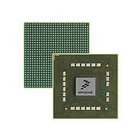
MPC8544VTALF Freescale Semiconductor, MPC8544VTALF Datasheet - Page 1257

MPC8544VTALF
Manufacturer Part Number
MPC8544VTALF
Description
MPU POWERQUICC III 783-PBGA
Manufacturer
Freescale Semiconductor
Datasheets
1.MPC8544VTALF.pdf
(117 pages)
2.MPC8544VTALF.pdf
(2 pages)
3.MPC8544VTALF.pdf
(1340 pages)
Specifications of MPC8544VTALF
Processor Type
MPC85xx PowerQUICC III 32-Bit
Speed
667MHz
Voltage
1V
Mounting Type
Surface Mount
Package / Case
783-FCPBGA
Processor Series
MPC85xx
Core
e500
Data Bus Width
32 bit
Maximum Clock Frequency
667 MHz
Maximum Operating Temperature
+ 105 C
Mounting Style
SMD/SMT
Data Ram Size
32 KB
I/o Voltage
1.8 V, 3.3 V
Interface Type
I2C, HSSI, DUART
Minimum Operating Temperature
0 C
Lead Free Status / RoHS Status
Lead free / RoHS Compliant
Features
-
Lead Free Status / Rohs Status
Lead free / RoHS Compliant
Available stocks
Company
Part Number
Manufacturer
Quantity
Price
Company:
Part Number:
MPC8544VTALF
Manufacturer:
Freescale Semiconductor
Quantity:
10 000
Company:
Part Number:
MPC8544VTALFA
Manufacturer:
Freescale Semiconductor
Quantity:
10 000
- Current page: 1257 of 1340
- Download datasheet (12Mb)
21.4.3
If MSRCID0 is low when sampled during POR, the LBC is selected as the source for the debug
information appearing on MSRCID[0:4] and MDVAL. For more information on this mode, see
Section 14.1.3.2, “Source ID Debug Mode.”
21.4.4
The watchpoint monitor (WM) can be programmed to arm and trigger on many different events including
any of the following:
A watchpoint event can be used in the following ways:
The large counters available in the performance monitor block and the interlock between it and the
watchpoint monitor support sophisticated debug scenarios.
A WM trigger event may be composed of several events programmed in the watchpoint monitor control
registers (WMCR0–WMCR1). Because the watchpoint monitor is disabled by default during POR, these
registers must be initialized to make use of this debug feature. Note that the WM address mask register
(WMAMR) and the type mask register (WMTMR) are cleared during POR. This means that the
watchpoint monitor’s default behavior following a power-on reset is to trigger on any address and no
transaction type. The reset value of WMCR0[TMD] is 0 which means transaction matching is enabled but
since no transaction is selected (WMTMR=0), a match will never occur. Either the transaction matching
must be disabled by setting WMCR0[TMD] to a value of 1, or valid transactions must be selected by
setting one or more of the WMTMR bits to a value of 1.
21.4.4.1
The WM can produce a performance monitor (PM) event with every trigger. This is accomplished by
configuring the performance monitor to count WM events. For more information on this configuration see
the events named ‘Number of watchpoint monitor hits’ and ‘Number of trace buffer hits’ in
Multi-level triggers can be created using the watchpoint monitor, the performance monitor, and the trace
buffer combined. For example, the WM can be programmed to trigger on events that also increment a PM
counter (the performance monitor must also be programmed to respond to this event), the output of which
(perfmon_overflow) could trigger the start of tracing in the trace buffer.
Freescale Semiconductor
•
•
•
•
•
•
•
External event (through TRIG_IN)
A trace buffer event
A performance monitor overflow event
A comparison of the current and programmed context ID registers
Trigger a logic analyzer (using TRIG_OUT)
Arm or trigger the trace buffer
Trigger a performance monitor event
Local Bus Interface Debug
Watchpoint Monitor
Watchpoint Monitor Performance Monitor Events
MPC8544E PowerQUICC III Integrated Host Processor Family Reference Manual, Rev. 1
Debug Features and Watchpoint Facility
Table
20-10.
21-27
Related parts for MPC8544VTALF
Image
Part Number
Description
Manufacturer
Datasheet
Request
R
Part Number:
Description:
Manufacturer:
Freescale Semiconductor, Inc
Datasheet:
Part Number:
Description:
Manufacturer:
Freescale Semiconductor, Inc
Datasheet:
Part Number:
Description:
Manufacturer:
Freescale Semiconductor, Inc
Datasheet:
Part Number:
Description:
Manufacturer:
Freescale Semiconductor, Inc
Datasheet:
Part Number:
Description:
Manufacturer:
Freescale Semiconductor, Inc
Datasheet:
Part Number:
Description:
Manufacturer:
Freescale Semiconductor, Inc
Datasheet:
Part Number:
Description:
Manufacturer:
Freescale Semiconductor, Inc
Datasheet:
Part Number:
Description:
Manufacturer:
Freescale Semiconductor, Inc
Datasheet:
Part Number:
Description:
Manufacturer:
Freescale Semiconductor, Inc
Datasheet:
Part Number:
Description:
Manufacturer:
Freescale Semiconductor, Inc
Datasheet:
Part Number:
Description:
Manufacturer:
Freescale Semiconductor, Inc
Datasheet:
Part Number:
Description:
Manufacturer:
Freescale Semiconductor, Inc
Datasheet:
Part Number:
Description:
Manufacturer:
Freescale Semiconductor, Inc
Datasheet:
Part Number:
Description:
Manufacturer:
Freescale Semiconductor, Inc
Datasheet:
Part Number:
Description:
Manufacturer:
Freescale Semiconductor, Inc
Datasheet:


