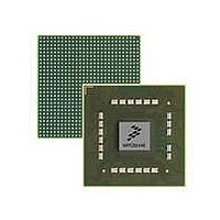
MPC8544VTALF Freescale Semiconductor, MPC8544VTALF Datasheet - Page 149

MPC8544VTALF
Manufacturer Part Number
MPC8544VTALF
Description
MPU POWERQUICC III 783-PBGA
Manufacturer
Freescale Semiconductor
Datasheets
1.MPC8544VTALF.pdf
(117 pages)
2.MPC8544VTALF.pdf
(2 pages)
3.MPC8544VTALF.pdf
(1340 pages)
Specifications of MPC8544VTALF
Processor Type
MPC85xx PowerQUICC III 32-Bit
Speed
667MHz
Voltage
1V
Mounting Type
Surface Mount
Package / Case
783-FCPBGA
Processor Series
MPC85xx
Core
e500
Data Bus Width
32 bit
Maximum Clock Frequency
667 MHz
Maximum Operating Temperature
+ 105 C
Mounting Style
SMD/SMT
Data Ram Size
32 KB
I/o Voltage
1.8 V, 3.3 V
Interface Type
I2C, HSSI, DUART
Minimum Operating Temperature
0 C
Lead Free Status / RoHS Status
Lead free / RoHS Compliant
Features
-
Lead Free Status / Rohs Status
Lead free / RoHS Compliant
Available stocks
Company
Part Number
Manufacturer
Quantity
Price
Company:
Part Number:
MPC8544VTALF
Manufacturer:
Freescale Semiconductor
Quantity:
10 000
Company:
Part Number:
MPC8544VTALFA
Manufacturer:
Freescale Semiconductor
Quantity:
10 000
- Current page: 149 of 1340
- Download datasheet (12Mb)
Freescale Semiconductor
SD1_REF_CLK,
SD2_REF_CLK,
SD1_REF_CLK
SD2_REF_CLK
HRESET_REQ
LSSD_MODE
SD1_RX[7:4],
SD1_TX[3:0],
SD1_TX[7:4],
SD2_RX[3:2],
SD2_TX[3:2],
CKSTP_OUT
MSRCID[2:4]
SD1_RX[7:4]
SD1_TX[3:0]
SD1_TX[7:4]
SD2_RX[3:2]
SD2_TX[3:2]
GPOUT[0:7]
L1_TSTCLK
SD2_RX[0],
SD2_TX[0],
SD2_RX[0]
TRIG_OUT
SD2_TX[0]
CKSTP_IN
MSRCID0
MSRCID1
GPIN[0:7]
HRESET
SRESET
TRIG_IN
ASLEEP
READY
MDVAL
Name
MPC8544E PowerQUICC III Integrated Host Processor Family Reference Manual, Rev. 1
Table 3-1. MPC8544E Signal Reference by Functional Block (continued)
Receive data,
receive data complement
Transmit data,
transmit data complement
Transmit data,
transmit data complement
SerDes1 reference clock,
SerDes1 reference clock
complement
Receive data,
receive data complement
Receive data,
receive data complement
Transmit data,
transmit data complement
Transmit data,
transmit data complement
SerDes2 reference clock,
SerDes2 reference clock
complement
Hard reset
Hard reset request
Soft reset
Checkstop in
Checkstop out
General-purpose output
General-purpose input
Device ready
Asleep
Watchpoint trigger in
Watchpoint trigger out
Memory debug source port ID 0
Memory debug source port ID 1
Memory debug source port ID
2–4
Memory debug data valid
LSSD mode
L1 test clock
Description
purpose outputs
PCI Express 1,
PCI Express 3,
System control
System control
System control
System control
System control
purpose inputs
System control
PCI Express 2
PCI Express 1
PCI Express 2
PCI Express 2
PCI Express 3
PCI Express 3
Power mgmt
Functional
General-
General-
Debug
Debug
Debug
Debug
Debug
Debug
Block
SGMII
SGMII
SGMII
Test
Test
Alternate Function(s)
cfg_mem_debug
cfg_ddr_debug
TRIG_OUT
READY
—
—
—
—
—
—
—
—
—
—
—
—
—
—
—
—
—
—
—
—
—
—
Signals
No. of
8
8
8
2
4
4
4
4
2
1
1
1
1
1
8
8
1
1
1
1
1
1
3
1
1
1
I/O
O
O
O
O
O
O
O
O
O
O
O
O
O
O
I
I
I
I
I
I
I
I
I
I
I
I
Signal Descriptions
19.4.1.9/19-12
19.4.1.9/19-12
19-2/19-2
19-2/19-2
19-2/19-2
19-2/19-2
19-2/19-2
21-4/21-8
21-4/21-8
21-3/21-7
21-3/21-7
21-3/21-7
21-3/21-7
21-5/21-8
21-5/21-8
4-2/4-2
4-2/4-2
4-2/4-2
4-2/4-2
Table/
Page
3-9
Related parts for MPC8544VTALF
Image
Part Number
Description
Manufacturer
Datasheet
Request
R
Part Number:
Description:
Manufacturer:
Freescale Semiconductor, Inc
Datasheet:
Part Number:
Description:
Manufacturer:
Freescale Semiconductor, Inc
Datasheet:
Part Number:
Description:
Manufacturer:
Freescale Semiconductor, Inc
Datasheet:
Part Number:
Description:
Manufacturer:
Freescale Semiconductor, Inc
Datasheet:
Part Number:
Description:
Manufacturer:
Freescale Semiconductor, Inc
Datasheet:
Part Number:
Description:
Manufacturer:
Freescale Semiconductor, Inc
Datasheet:
Part Number:
Description:
Manufacturer:
Freescale Semiconductor, Inc
Datasheet:
Part Number:
Description:
Manufacturer:
Freescale Semiconductor, Inc
Datasheet:
Part Number:
Description:
Manufacturer:
Freescale Semiconductor, Inc
Datasheet:
Part Number:
Description:
Manufacturer:
Freescale Semiconductor, Inc
Datasheet:
Part Number:
Description:
Manufacturer:
Freescale Semiconductor, Inc
Datasheet:
Part Number:
Description:
Manufacturer:
Freescale Semiconductor, Inc
Datasheet:
Part Number:
Description:
Manufacturer:
Freescale Semiconductor, Inc
Datasheet:
Part Number:
Description:
Manufacturer:
Freescale Semiconductor, Inc
Datasheet:
Part Number:
Description:
Manufacturer:
Freescale Semiconductor, Inc
Datasheet:


