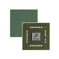
MPC8544VTALF Freescale Semiconductor, MPC8544VTALF Datasheet - Page 211

MPC8544VTALF
Manufacturer Part Number
MPC8544VTALF
Description
MPU POWERQUICC III 783-PBGA
Manufacturer
Freescale Semiconductor
Datasheets
1.MPC8544VTALF.pdf
(117 pages)
2.MPC8544VTALF.pdf
(2 pages)
3.MPC8544VTALF.pdf
(1340 pages)
Specifications of MPC8544VTALF
Processor Type
MPC85xx PowerQUICC III 32-Bit
Speed
667MHz
Voltage
1V
Mounting Type
Surface Mount
Package / Case
783-FCPBGA
Processor Series
MPC85xx
Core
e500
Data Bus Width
32 bit
Maximum Clock Frequency
667 MHz
Maximum Operating Temperature
+ 105 C
Mounting Style
SMD/SMT
Data Ram Size
32 KB
I/o Voltage
1.8 V, 3.3 V
Interface Type
I2C, HSSI, DUART
Minimum Operating Temperature
0 C
Lead Free Status / RoHS Status
Lead free / RoHS Compliant
Features
-
Lead Free Status / Rohs Status
Lead free / RoHS Compliant
Available stocks
Company
Part Number
Manufacturer
Quantity
Price
Company:
Part Number:
MPC8544VTALF
Manufacturer:
Freescale Semiconductor
Quantity:
10 000
Company:
Part Number:
MPC8544VTALFA
Manufacturer:
Freescale Semiconductor
Quantity:
10 000
- Current page: 211 of 1340
- Download datasheet (12Mb)
Figure 5-10
The appropriate L1 MMU (instruction or data) is checked for a matching address translation. The
instruction L1 MMU and data L1 MMU operate independently and can be accessed in parallel, so that hits
for instruction accesses and data accesses can occur in the same clock. If an L1 MMU misses, the request
for translation is forwarded to the unified (instruction and data) L2 MMU. If found, the contents of the
TLB entry are concatenated with the byte address to obtain the physical address of the requested access.
On misses, the L1 TLB entries are replaced from their L2 TLB counterparts using a true LRU algorithm.
5.9.2
MMU assist registers are used to hold values either read from or to be written to the TLBs and information
required to identify the TLB to be accessed. MAS3 implements the real page number (RPN), the user
attribute bits (U0–U3), and permission bits (UX, SX, UW, SW, UR, SR) that specify user and supervisor
read, write, and execute permissions.
The e500 does not implement MAS5.
Freescale Semiconductor
Instruction Access
512-Entry 4-Way Set Assoc. Array (TLB0)
* Number of bits depends on page size
16-Entry Fully-Assoc. VSP Array (TLB1)
shows the same translation flow for the e500v2 core.
MMU Assist Registers (MAS0–MAS4 and MAS6–MAS7)
MPC8544E PowerQUICC III Integrated Host Processor Family Reference Manual, Rev. 1
(4 Kbytes–4 Gbytes)
•••
Figure 5-10. Effective-to-Real Address Translation Flow (e500v2)
L2 MMU (unified)
IS DS •••
36-bit Real Address
Data Access
AS
MSR
8 bits
PID0
PID2
PID1
4–24 bits*
0–20 bits*
Three 41-bit Virtual Addresses (VAs)
Instruction L1 MMU
Real Page Number
Effective Page Number
2 TLBs
L1 MMUs
32-bit Effective Address (EA)
Data L1 MMU
2 TLBs
12–32 bits*
12–32 bits*
Byte Address
Byte Address
Core Complex Overview
5-25
Related parts for MPC8544VTALF
Image
Part Number
Description
Manufacturer
Datasheet
Request
R
Part Number:
Description:
Manufacturer:
Freescale Semiconductor, Inc
Datasheet:
Part Number:
Description:
Manufacturer:
Freescale Semiconductor, Inc
Datasheet:
Part Number:
Description:
Manufacturer:
Freescale Semiconductor, Inc
Datasheet:
Part Number:
Description:
Manufacturer:
Freescale Semiconductor, Inc
Datasheet:
Part Number:
Description:
Manufacturer:
Freescale Semiconductor, Inc
Datasheet:
Part Number:
Description:
Manufacturer:
Freescale Semiconductor, Inc
Datasheet:
Part Number:
Description:
Manufacturer:
Freescale Semiconductor, Inc
Datasheet:
Part Number:
Description:
Manufacturer:
Freescale Semiconductor, Inc
Datasheet:
Part Number:
Description:
Manufacturer:
Freescale Semiconductor, Inc
Datasheet:
Part Number:
Description:
Manufacturer:
Freescale Semiconductor, Inc
Datasheet:
Part Number:
Description:
Manufacturer:
Freescale Semiconductor, Inc
Datasheet:
Part Number:
Description:
Manufacturer:
Freescale Semiconductor, Inc
Datasheet:
Part Number:
Description:
Manufacturer:
Freescale Semiconductor, Inc
Datasheet:
Part Number:
Description:
Manufacturer:
Freescale Semiconductor, Inc
Datasheet:
Part Number:
Description:
Manufacturer:
Freescale Semiconductor, Inc
Datasheet:


