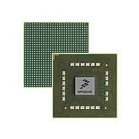
MPC8544VTALF Freescale Semiconductor, MPC8544VTALF Datasheet - Page 745

MPC8544VTALF
Manufacturer Part Number
MPC8544VTALF
Description
MPU POWERQUICC III 783-PBGA
Manufacturer
Freescale Semiconductor
Datasheets
1.MPC8544VTALF.pdf
(117 pages)
2.MPC8544VTALF.pdf
(2 pages)
3.MPC8544VTALF.pdf
(1340 pages)
Specifications of MPC8544VTALF
Processor Type
MPC85xx PowerQUICC III 32-Bit
Speed
667MHz
Voltage
1V
Mounting Type
Surface Mount
Package / Case
783-FCPBGA
Processor Series
MPC85xx
Core
e500
Data Bus Width
32 bit
Maximum Clock Frequency
667 MHz
Maximum Operating Temperature
+ 105 C
Mounting Style
SMD/SMT
Data Ram Size
32 KB
I/o Voltage
1.8 V, 3.3 V
Interface Type
I2C, HSSI, DUART
Minimum Operating Temperature
0 C
Lead Free Status / RoHS Status
Lead free / RoHS Compliant
Features
-
Lead Free Status / Rohs Status
Lead free / RoHS Compliant
Available stocks
Company
Part Number
Manufacturer
Quantity
Price
Company:
Part Number:
MPC8544VTALF
Manufacturer:
Freescale Semiconductor
Quantity:
10 000
Company:
Part Number:
MPC8544VTALFA
Manufacturer:
Freescale Semiconductor
Quantity:
10 000
- Current page: 745 of 1340
- Download datasheet (12Mb)
15.5
The eTSECs use a software model that is a superset of the PowerQUICC III TSEC functionality and is
similar to that employed by the Fast Ethernet function supported on the Freescale MPC8260 CPM FCC
and in the FEC of the MPC860T.
The eTSEC device is programmed by a combination of control/status registers (CSRs) and buffer
descriptors. The CSRs are used for mode control, interrupts, and to extract status information. The
descriptors are used to pass data buffers and related buffer status or frame information between the
hardware and software.
All accesses to and from the registers must be made as 32-bit accesses. There is no support for accesses of
sizes other than 32 bits. Writes to reserved register bits must always store 0, as writing 1 to reserved bits
may have unintended side-effects. Reads from unmapped register addresses return zero. Unless otherwise
specified, the read value of reserved bits in mapped registers is not defined, and must not be assumed to
be 0.
This section of the document defines the memory map and describes the registers in detail. The buffer
descriptor is described in
The ten-bit interface (TBI) module MII registers are also described in this section. The TBI registers are
defined like PHY registers and, as such, are accessed via the MII management interface in the same way
the PHYs are accessed. For detailed descriptions of the TBI registers (the MII register set for the ten-bit
interface) refer to
15.5.1
Each of the two eTSECs is allocated 4 Kbytes of memory-mapped space. The space for each eTSEC is
divided as indicated in
Freescale Semiconductor
Memory Map/Register Definition
Top-Level Module Memory Map
MPC8544E PowerQUICC III Integrated Host Processor Family Reference Manual, Rev. 1
Section 15.5.4, “Ten-Bit Interface (TBI).”
Table
Section 15.6.7, “Buffer Descriptors.”
Address Offset
C00–C3F
A00–AFF
B00–BFF
15-3.
000–0FF
100–2FF
300–4FF
500–5FF
600–7FF
800–8FF
900–9FF
C–FFF
Table 15-3. Module Memory Map Summary
eTSEC general control/status registers
eTSEC transmit control/status registers
eTSEC receive control/status registers
MAC registers
RMON MIB registers
Hash table registers
—
FIFO control/status registers
DMA system registers
Lossless Flow Control registers
—
Function
Enhanced Three-Speed Ethernet Controllers
15-13
Related parts for MPC8544VTALF
Image
Part Number
Description
Manufacturer
Datasheet
Request
R
Part Number:
Description:
Manufacturer:
Freescale Semiconductor, Inc
Datasheet:
Part Number:
Description:
Manufacturer:
Freescale Semiconductor, Inc
Datasheet:
Part Number:
Description:
Manufacturer:
Freescale Semiconductor, Inc
Datasheet:
Part Number:
Description:
Manufacturer:
Freescale Semiconductor, Inc
Datasheet:
Part Number:
Description:
Manufacturer:
Freescale Semiconductor, Inc
Datasheet:
Part Number:
Description:
Manufacturer:
Freescale Semiconductor, Inc
Datasheet:
Part Number:
Description:
Manufacturer:
Freescale Semiconductor, Inc
Datasheet:
Part Number:
Description:
Manufacturer:
Freescale Semiconductor, Inc
Datasheet:
Part Number:
Description:
Manufacturer:
Freescale Semiconductor, Inc
Datasheet:
Part Number:
Description:
Manufacturer:
Freescale Semiconductor, Inc
Datasheet:
Part Number:
Description:
Manufacturer:
Freescale Semiconductor, Inc
Datasheet:
Part Number:
Description:
Manufacturer:
Freescale Semiconductor, Inc
Datasheet:
Part Number:
Description:
Manufacturer:
Freescale Semiconductor, Inc
Datasheet:
Part Number:
Description:
Manufacturer:
Freescale Semiconductor, Inc
Datasheet:
Part Number:
Description:
Manufacturer:
Freescale Semiconductor, Inc
Datasheet:


