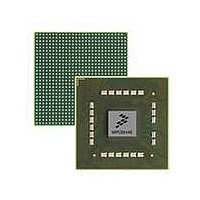
MPC8544VTALF Freescale Semiconductor, MPC8544VTALF Datasheet - Page 286

MPC8544VTALF
Manufacturer Part Number
MPC8544VTALF
Description
MPU POWERQUICC III 783-PBGA
Manufacturer
Freescale Semiconductor
Datasheets
1.MPC8544VTALF.pdf
(117 pages)
2.MPC8544VTALF.pdf
(2 pages)
3.MPC8544VTALF.pdf
(1340 pages)
Specifications of MPC8544VTALF
Processor Type
MPC85xx PowerQUICC III 32-Bit
Speed
667MHz
Voltage
1V
Mounting Type
Surface Mount
Package / Case
783-FCPBGA
Processor Series
MPC85xx
Core
e500
Data Bus Width
32 bit
Maximum Clock Frequency
667 MHz
Maximum Operating Temperature
+ 105 C
Mounting Style
SMD/SMT
Data Ram Size
32 KB
I/o Voltage
1.8 V, 3.3 V
Interface Type
I2C, HSSI, DUART
Minimum Operating Temperature
0 C
Lead Free Status / RoHS Status
Lead free / RoHS Compliant
Features
-
Lead Free Status / Rohs Status
Lead free / RoHS Compliant
Available stocks
Company
Part Number
Manufacturer
Quantity
Price
Company:
Part Number:
MPC8544VTALF
Manufacturer:
Freescale Semiconductor
Quantity:
10 000
Company:
Part Number:
MPC8544VTALFA
Manufacturer:
Freescale Semiconductor
Quantity:
10 000
- Current page: 286 of 1340
- Download datasheet (12Mb)
L2 Look-Aside Cache/SRAM
7.3.1.3.1
The L2 memory-mapped SRAM base address registers (L2SRBARn), shown in
lower 18 bits of the 22-bit SRAM base address.
L2SRBAR bits are described in
When enabled, the windows defined in L2SRBARn and L2SRBAREAn supersede all other mappings of
these addresses for processor and global (snoopable) I/O transactions. Therefore, SRAM windows must
never overlap configuration space as defined by CCSRBAR (see
Control, and Status Base Address Register
is discouraged because processor and snoopable I/O transactions would map to the SRAM while
non-snooped I/O transactions would be mapped by the local access windows. Only if all accesses to the
SRAM address range are snoopable can results be consistent if SRAM and local access windows overlap.
7-16
18–31
Offset 0x2_0100
0–17
Reset
Bits
W
R
0x2_0108
0
ADDR Contains the lower 18 bits of the 22-bit L2 memory-mapped SRAM base address; the upper 4 bits are
Name
—
MPC8544E PowerQUICC III Integrated Host Processor Family Reference Manual, Rev. 1
Figure 7-11. L2 Memory-Mapped SRAM Base Address Registers (L2SRBAR n )
contained in L2SRBAREA n [ADDR]. (Note that some of these bits may not be needed, depending on how the
L2 cache is partitioned.) The combined base address from L2SRBAREA n [ADDR] || L2SRBAR n [ADDR] is
used as follows:
SRAM Partition
64 Kbytes
128 Kbytes
256 Kbytes
Unused bits of the base address are masked off by the hardware.
Reserved
L2 Memory-Mapped SRAM Base Address Registers 0–1 (L2SRBAR n )
Bits Required for SRAM Offset
ADDR
Table
Table 7-8. L2SRBAR n Field Descriptions
16
17
18
7-8.
(CCSRBAR).”) Overlapping SRAM and local access windows
All zeros
Description
17 18
Bits Used for Actual Base Address
20 (0–19)
19 (0–18)
18 (0–17)
Section 4.3.1.1.2, “Configuration,
Figure
—
Freescale Semiconductor
Access: Read/Write
7-11, contain the
31
Related parts for MPC8544VTALF
Image
Part Number
Description
Manufacturer
Datasheet
Request
R
Part Number:
Description:
Manufacturer:
Freescale Semiconductor, Inc
Datasheet:
Part Number:
Description:
Manufacturer:
Freescale Semiconductor, Inc
Datasheet:
Part Number:
Description:
Manufacturer:
Freescale Semiconductor, Inc
Datasheet:
Part Number:
Description:
Manufacturer:
Freescale Semiconductor, Inc
Datasheet:
Part Number:
Description:
Manufacturer:
Freescale Semiconductor, Inc
Datasheet:
Part Number:
Description:
Manufacturer:
Freescale Semiconductor, Inc
Datasheet:
Part Number:
Description:
Manufacturer:
Freescale Semiconductor, Inc
Datasheet:
Part Number:
Description:
Manufacturer:
Freescale Semiconductor, Inc
Datasheet:
Part Number:
Description:
Manufacturer:
Freescale Semiconductor, Inc
Datasheet:
Part Number:
Description:
Manufacturer:
Freescale Semiconductor, Inc
Datasheet:
Part Number:
Description:
Manufacturer:
Freescale Semiconductor, Inc
Datasheet:
Part Number:
Description:
Manufacturer:
Freescale Semiconductor, Inc
Datasheet:
Part Number:
Description:
Manufacturer:
Freescale Semiconductor, Inc
Datasheet:
Part Number:
Description:
Manufacturer:
Freescale Semiconductor, Inc
Datasheet:
Part Number:
Description:
Manufacturer:
Freescale Semiconductor, Inc
Datasheet:


