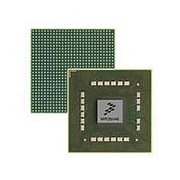
MPC8544VTALF Freescale Semiconductor, MPC8544VTALF Datasheet - Page 650

MPC8544VTALF
Manufacturer Part Number
MPC8544VTALF
Description
MPU POWERQUICC III 783-PBGA
Manufacturer
Freescale Semiconductor
Datasheets
1.MPC8544VTALF.pdf
(117 pages)
2.MPC8544VTALF.pdf
(2 pages)
3.MPC8544VTALF.pdf
(1340 pages)
Specifications of MPC8544VTALF
Processor Type
MPC85xx PowerQUICC III 32-Bit
Speed
667MHz
Voltage
1V
Mounting Type
Surface Mount
Package / Case
783-FCPBGA
Processor Series
MPC85xx
Core
e500
Data Bus Width
32 bit
Maximum Clock Frequency
667 MHz
Maximum Operating Temperature
+ 105 C
Mounting Style
SMD/SMT
Data Ram Size
32 KB
I/o Voltage
1.8 V, 3.3 V
Interface Type
I2C, HSSI, DUART
Minimum Operating Temperature
0 C
Lead Free Status / RoHS Status
Lead free / RoHS Compliant
Features
-
Lead Free Status / Rohs Status
Lead free / RoHS Compliant
Available stocks
Company
Part Number
Manufacturer
Quantity
Price
Company:
Part Number:
MPC8544VTALF
Manufacturer:
Freescale Semiconductor
Quantity:
10 000
Company:
Part Number:
MPC8544VTALFA
Manufacturer:
Freescale Semiconductor
Quantity:
10 000
- Current page: 650 of 1340
- Download datasheet (12Mb)
Local Bus Controller
14.3.1.16
The clock ratio register sets the system (CCB) clock to LBC bus frequency ratio. It also provides
configuration bits for extra delay cycles for address and control signals.
14-30
11–13
16–23
24–31
Bits
8–9
10
14
15
Offset 0x0D4
Reset
W
R
BCTLC Defines the use of LBCTL
LPBSE Enables parity byte select on LGTA/LGPL4/LUPWAIT/LPBSE signal.
Name
EPAR Determines odd or even parity. Writing the memory with EPAR = 1 and reading the memory with EPAR = 0
AHD
BMT
PBYP — BUFCMDC
—
—
1
0
MPC8544E PowerQUICC III Integrated Host Processor Family Reference Manual, Rev. 1
Clock Ratio Register (LCRR)
00 LBCTL is used as W/R control for GPCM or UPM accesses (buffer control).
01 LBCTL is used as LOE for GPCM accesses only.
10 LBCTL is used as LWE for GPCM accesses only.
11 Reserved.
Address hold disable. Removes part of the hold time for LAD with respect to LALE in order to lengthen the
LALE pulse
0 During address phases on the local bus, the LALE signal negates two platform clock periods prior to the
1 During address phases on the local bus, the LALE signal negates one platform clock period prior to the
Reserved
0 Parity byte select is disabled. LGTA/LGPL4/LUPWAIT/LPBSE signal is available for memory control as
1 Parity byte select is enabled. LGTA/LGPL4/LUPWAIT/LPBSE signal is dedicated as the parity byte select
generates parity errors for testing.
0 Odd parity
1 Even parity
Bus monitor timing. Defines the bus monitor time-out period. Clearing BMT (reset value) selects the maximum
count of 2048 bus clock cycles. For non-zero values of BMT, the number of LCLK clock cycles to count down
before a time-out error is generated is given by: bus cycles = BMT x 8.
Apart from BMT = 0x00, the minimum value of BMT is 5, corresponding with 40 bus cycles. Shorter time-outs
may result in spurious errors during SDRAM operation.
Reserved
1
0
address being invalidated. At 666 MHz, this provides 3 ns of additional address hold time at the external
address latch.
address being invalidated. This halves the address hold time, but extends the latch enable duration. This
may be necessary for very high frequency designs.
LGPL4 (output) or LGTA/LUPWAIT (input).
output, and LGTA/LUPWAIT is disabled.
0
2
0
3
Table 14-21. LBCR Field Descriptions (continued)
0 0 0 0 0 0 0 0 0 0 0
4
—
Figure 14-19. Clock Ratio Register (LCRR)
5
6
ECL
7
8
—
13 14 15 16
Description
EADC
0 0 0 0 0 0 0 0 0 0 0 0 0 1 0 0 0
—
Freescale Semiconductor
Access: Read/Write
27 28
CLKDIV
31
Related parts for MPC8544VTALF
Image
Part Number
Description
Manufacturer
Datasheet
Request
R
Part Number:
Description:
Manufacturer:
Freescale Semiconductor, Inc
Datasheet:
Part Number:
Description:
Manufacturer:
Freescale Semiconductor, Inc
Datasheet:
Part Number:
Description:
Manufacturer:
Freescale Semiconductor, Inc
Datasheet:
Part Number:
Description:
Manufacturer:
Freescale Semiconductor, Inc
Datasheet:
Part Number:
Description:
Manufacturer:
Freescale Semiconductor, Inc
Datasheet:
Part Number:
Description:
Manufacturer:
Freescale Semiconductor, Inc
Datasheet:
Part Number:
Description:
Manufacturer:
Freescale Semiconductor, Inc
Datasheet:
Part Number:
Description:
Manufacturer:
Freescale Semiconductor, Inc
Datasheet:
Part Number:
Description:
Manufacturer:
Freescale Semiconductor, Inc
Datasheet:
Part Number:
Description:
Manufacturer:
Freescale Semiconductor, Inc
Datasheet:
Part Number:
Description:
Manufacturer:
Freescale Semiconductor, Inc
Datasheet:
Part Number:
Description:
Manufacturer:
Freescale Semiconductor, Inc
Datasheet:
Part Number:
Description:
Manufacturer:
Freescale Semiconductor, Inc
Datasheet:
Part Number:
Description:
Manufacturer:
Freescale Semiconductor, Inc
Datasheet:
Part Number:
Description:
Manufacturer:
Freescale Semiconductor, Inc
Datasheet:


