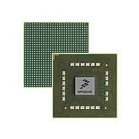
MPC8544VTALF Freescale Semiconductor, MPC8544VTALF Datasheet - Page 642

MPC8544VTALF
Manufacturer Part Number
MPC8544VTALF
Description
MPU POWERQUICC III 783-PBGA
Manufacturer
Freescale Semiconductor
Datasheets
1.MPC8544VTALF.pdf
(117 pages)
2.MPC8544VTALF.pdf
(2 pages)
3.MPC8544VTALF.pdf
(1340 pages)
Specifications of MPC8544VTALF
Processor Type
MPC85xx PowerQUICC III 32-Bit
Speed
667MHz
Voltage
1V
Mounting Type
Surface Mount
Package / Case
783-FCPBGA
Processor Series
MPC85xx
Core
e500
Data Bus Width
32 bit
Maximum Clock Frequency
667 MHz
Maximum Operating Temperature
+ 105 C
Mounting Style
SMD/SMT
Data Ram Size
32 KB
I/o Voltage
1.8 V, 3.3 V
Interface Type
I2C, HSSI, DUART
Minimum Operating Temperature
0 C
Lead Free Status / RoHS Status
Lead free / RoHS Compliant
Features
-
Lead Free Status / Rohs Status
Lead free / RoHS Compliant
Available stocks
Company
Part Number
Manufacturer
Quantity
Price
Company:
Part Number:
MPC8544VTALF
Manufacturer:
Freescale Semiconductor
Quantity:
10 000
Company:
Part Number:
MPC8544VTALFA
Manufacturer:
Freescale Semiconductor
Quantity:
10 000
- Current page: 642 of 1340
- Download datasheet (12Mb)
Local Bus Controller
14-22
14–16
17–19
20–22
24–25
26–27
30–31
Bits
23
28
29
PRETOACT Defines the earliest timing for ACTIVATE or REFRESH command after a PRECHARGE command
ACTTORW Defines the earliest timing for READ/WRITE command after an ACTIVATE command (number of bus
BUFCMD
Name
RFCR
WRC
CL
BL
—
—
MPC8544E PowerQUICC III Integrated Host Processor Family Reference Manual, Rev. 1
Refresh recovery. Sets the refresh recovery interval in bus clock cycles. Defines the earliest timing for
an ACTIVATE or REFRESH command after a REFRESH command.
000 Reserved
001 3 clocks
010 4 clocks
011 5 clocks
(number of bus clock cycle wait states).
000 8
001 1
010 2
011 3
clock cycle wait states).
000 8
001 Reserved
010 2
011 3
Sets the burst length for SDRAM accesses.
0 SDRAM burst length is 4. Use this value if the device port size is16.
1 SDRAM burst length is 8. Use this value if the device port size is 32 or 8.
Reserved
Write recovery time. Defines the earliest timing for PRECHARGE command after the last data is written
to the SDRAM.
00 4
01 Reserved
10 2
11 3
Reserved
Control line assertion timing. If external buffers are placed on the control lines going to both the SDRAM
and address lines, setting BUFCMD causes all SDRAM control lines except LCS n , LCKE, LALE, and
LSDDQM[0:3] to be asserted for LCRR[BUFCMDC] cycles, instead of one.
0 Normal timing for the control lines
1 All control lines except LCS n are asserted for the number of cycles specified by LCRR[BUFCMDC].
CAS latency. Defines the timing for first read data after SDRAM samples a column address.
00 Extended CAS latency. According to LCRR[ECL]. See
01 1
10 2
11 3
Table 14-13. LSDMR Field Descriptions (continued)
100 6 clocks
101 7 clocks
110 8 clocks
111 16 clocks
100 4
101 5
110 6
111 7
100 4
101 5
110 6
111 7
Description
Table
14-22.
Freescale Semiconductor
Related parts for MPC8544VTALF
Image
Part Number
Description
Manufacturer
Datasheet
Request
R
Part Number:
Description:
Manufacturer:
Freescale Semiconductor, Inc
Datasheet:
Part Number:
Description:
Manufacturer:
Freescale Semiconductor, Inc
Datasheet:
Part Number:
Description:
Manufacturer:
Freescale Semiconductor, Inc
Datasheet:
Part Number:
Description:
Manufacturer:
Freescale Semiconductor, Inc
Datasheet:
Part Number:
Description:
Manufacturer:
Freescale Semiconductor, Inc
Datasheet:
Part Number:
Description:
Manufacturer:
Freescale Semiconductor, Inc
Datasheet:
Part Number:
Description:
Manufacturer:
Freescale Semiconductor, Inc
Datasheet:
Part Number:
Description:
Manufacturer:
Freescale Semiconductor, Inc
Datasheet:
Part Number:
Description:
Manufacturer:
Freescale Semiconductor, Inc
Datasheet:
Part Number:
Description:
Manufacturer:
Freescale Semiconductor, Inc
Datasheet:
Part Number:
Description:
Manufacturer:
Freescale Semiconductor, Inc
Datasheet:
Part Number:
Description:
Manufacturer:
Freescale Semiconductor, Inc
Datasheet:
Part Number:
Description:
Manufacturer:
Freescale Semiconductor, Inc
Datasheet:
Part Number:
Description:
Manufacturer:
Freescale Semiconductor, Inc
Datasheet:
Part Number:
Description:
Manufacturer:
Freescale Semiconductor, Inc
Datasheet:


