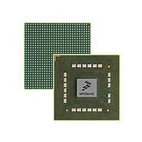
MPC8544VTALF Freescale Semiconductor, MPC8544VTALF Datasheet - Page 193

MPC8544VTALF
Manufacturer Part Number
MPC8544VTALF
Description
MPU POWERQUICC III 783-PBGA
Manufacturer
Freescale Semiconductor
Datasheets
1.MPC8544VTALF.pdf
(117 pages)
2.MPC8544VTALF.pdf
(2 pages)
3.MPC8544VTALF.pdf
(1340 pages)
Specifications of MPC8544VTALF
Processor Type
MPC85xx PowerQUICC III 32-Bit
Speed
667MHz
Voltage
1V
Mounting Type
Surface Mount
Package / Case
783-FCPBGA
Processor Series
MPC85xx
Core
e500
Data Bus Width
32 bit
Maximum Clock Frequency
667 MHz
Maximum Operating Temperature
+ 105 C
Mounting Style
SMD/SMT
Data Ram Size
32 KB
I/o Voltage
1.8 V, 3.3 V
Interface Type
I2C, HSSI, DUART
Minimum Operating Temperature
0 C
Lead Free Status / RoHS Status
Lead free / RoHS Compliant
Features
-
Lead Free Status / Rohs Status
Lead free / RoHS Compliant
Available stocks
Company
Part Number
Manufacturer
Quantity
Price
Company:
Part Number:
MPC8544VTALF
Manufacturer:
Freescale Semiconductor
Quantity:
10 000
Company:
Part Number:
MPC8544VTALFA
Manufacturer:
Freescale Semiconductor
Quantity:
10 000
- Current page: 193 of 1340
- Download datasheet (12Mb)
Freescale Semiconductor
•
•
•
•
•
Completion unit
— As many as 14 instructions allowed in 14-entry completion queue (CQ)
— In-order retirement of as many as two instructions per cycle
— Completion and refetch serialization control
— Synchronization for all instruction flow changes—interrupts, mispredicted branches, and
Issue queues
— Two-entry branch instruction issue queue (BIQ)
— Four-entry general instruction issue queue (GIQ)
Branch unit—The branch unit (BU) is an execution unit and is distinct from the BPU. It executes
(resolves) all branch and CR logical instructions.
Two simple units (SU1 and SU2)
— Add and subtract
— Shift and rotate
— Logical operations
— Support for 64-bit SPE instructions in SU1
Multiple-cycle unit (MU)—The MU is shown in
The MU has the following features:
— Four-cycle latency for all multiplication, including SPE integer and fractional multiply
— Variable-latency divide: 4, 11, 19, and 35 cycles for all integer divide instructions. If rA or rB
context-synchronizing instructions
instructions and embedded scalar and vector floating-point multiply instructions
is zero, floating-point divide instructions take 4 cycles; all others take 29. Note that although
most divide instructions take more than 4 cycles to execute, the MU allows subsequent
multiply instructions to execute through all four MU stages in parallel with the divide.
MPC8544E PowerQUICC III Integrated Host Processor Family Reference Manual, Rev. 1
Figure 5-3. Four-Stage MU Pipeline, Showing Divide Bypass
Upper
Reservation
Station
MU-1
MU-2
MU-3
MU-4
Lower
From GIQ0 or GIQ1
Divide Bypass Path
Postdivide
Divide
Figure
5-3.
Core Complex Overview
5-7
Related parts for MPC8544VTALF
Image
Part Number
Description
Manufacturer
Datasheet
Request
R
Part Number:
Description:
Manufacturer:
Freescale Semiconductor, Inc
Datasheet:
Part Number:
Description:
Manufacturer:
Freescale Semiconductor, Inc
Datasheet:
Part Number:
Description:
Manufacturer:
Freescale Semiconductor, Inc
Datasheet:
Part Number:
Description:
Manufacturer:
Freescale Semiconductor, Inc
Datasheet:
Part Number:
Description:
Manufacturer:
Freescale Semiconductor, Inc
Datasheet:
Part Number:
Description:
Manufacturer:
Freescale Semiconductor, Inc
Datasheet:
Part Number:
Description:
Manufacturer:
Freescale Semiconductor, Inc
Datasheet:
Part Number:
Description:
Manufacturer:
Freescale Semiconductor, Inc
Datasheet:
Part Number:
Description:
Manufacturer:
Freescale Semiconductor, Inc
Datasheet:
Part Number:
Description:
Manufacturer:
Freescale Semiconductor, Inc
Datasheet:
Part Number:
Description:
Manufacturer:
Freescale Semiconductor, Inc
Datasheet:
Part Number:
Description:
Manufacturer:
Freescale Semiconductor, Inc
Datasheet:
Part Number:
Description:
Manufacturer:
Freescale Semiconductor, Inc
Datasheet:
Part Number:
Description:
Manufacturer:
Freescale Semiconductor, Inc
Datasheet:
Part Number:
Description:
Manufacturer:
Freescale Semiconductor, Inc
Datasheet:


