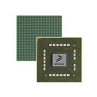
MPC8544VTALF Freescale Semiconductor, MPC8544VTALF Datasheet - Page 212

MPC8544VTALF
Manufacturer Part Number
MPC8544VTALF
Description
MPU POWERQUICC III 783-PBGA
Manufacturer
Freescale Semiconductor
Datasheets
1.MPC8544VTALF.pdf
(117 pages)
2.MPC8544VTALF.pdf
(2 pages)
3.MPC8544VTALF.pdf
(1340 pages)
Specifications of MPC8544VTALF
Processor Type
MPC85xx PowerQUICC III 32-Bit
Speed
667MHz
Voltage
1V
Mounting Type
Surface Mount
Package / Case
783-FCPBGA
Processor Series
MPC85xx
Core
e500
Data Bus Width
32 bit
Maximum Clock Frequency
667 MHz
Maximum Operating Temperature
+ 105 C
Mounting Style
SMD/SMT
Data Ram Size
32 KB
I/o Voltage
1.8 V, 3.3 V
Interface Type
I2C, HSSI, DUART
Minimum Operating Temperature
0 C
Lead Free Status / RoHS Status
Lead free / RoHS Compliant
Features
-
Lead Free Status / Rohs Status
Lead free / RoHS Compliant
Available stocks
Company
Part Number
Manufacturer
Quantity
Price
Company:
Part Number:
MPC8544VTALF
Manufacturer:
Freescale Semiconductor
Quantity:
10 000
Company:
Part Number:
MPC8544VTALFA
Manufacturer:
Freescale Semiconductor
Quantity:
10 000
- Current page: 212 of 1340
- Download datasheet (12Mb)
Core Complex Overview
MAS registers are affected by the following instructions (see for more detailed information):
For TLB miss and certain MMU-related DSI/ISI exceptions, MAS4 provides default values for updating
MAS0–MAS2.
5.9.3
The e500 core complex also implements three process ID (PID) registers that hold the values used to
construct the three virtual addresses for each access. These process IDs provide an extended page sharing
capability. Which of these three virtual addresses is used is controlled by the TID field of a matching TLB
entry, and when TID = 0x00 (identifying a page as globally shared), the PID values are ignored.
A hit to multiple TLB entries in the L1 MMU (even if they are in separate arrays) or a hit to multiple entries
in the L2 MMU is considered to be a programming error.
5.9.4
The core complex provides the ability to invalidate a TLB entry, as defined by the architecture. The tlbivax
instruction invalidates a matching local TLB entry. Execution of this instruction is also broadcast on the
core complex bus (CCB) if HID1[ABE] is set. The core complex also snoops TLB invalidate transactions
on the CCB from other bus masters.
5.10
The core complex supports four-state memory coherency. Memory coherency is hardware-supported on
the system bus through bus snooping and the retry/copyback bus protocol, and through broadcasting of
cache management instructions. Translation coherency is also hardware-supported through broadcasting
and bus snooping of TLB invalidate transactions. The four-state MESI protocol supports efficient
large-scale real-time data sharing between multiple caching bus masters.
5.10.1
The e500 core supports atomic update memory references for both aligned word forms of data using the
load and reserve and store conditional instruction pair, lwarx and stwcx. Typically, a load and reserve
5-26
•
•
•
•
MAS registers are accessed with the mtspr and mfspr instructions.
The TLB Read Entry instruction (tlbre) causes the contents of a single TLB entry from the L2
MMU to be placed in defined locations in MAS0–MAS3 (and optionally MAS7 on the e500v2).
The TLB entry to be extracted is determined by information written to MAS0 and MAS2 before
the tlbre instruction is executed.
The TLB Write Entry instruction (tlbwe) causes the information stored in certain locations of
MAS0–MAS3 (and MAS7 on the e500v2) to be written to the TLB specified in MAS0.
The TLB Search Indexed instruction (tlbsx) updates MAS registers conditionally, based on success
or failure of a lookup in the L2 MMU. The lookup is specified by the instruction encoding and
specific search fields in MAS6. The values placed in the MAS registers may differ, depending on
a successful or unsuccessful search.
Memory Coherency
Process ID Registers (PID0–PID2)
TLB Coherency
Atomic Update Memory References
MPC8544E PowerQUICC III Integrated Host Processor Family Reference Manual, Rev. 1
Freescale Semiconductor
Related parts for MPC8544VTALF
Image
Part Number
Description
Manufacturer
Datasheet
Request
R
Part Number:
Description:
Manufacturer:
Freescale Semiconductor, Inc
Datasheet:
Part Number:
Description:
Manufacturer:
Freescale Semiconductor, Inc
Datasheet:
Part Number:
Description:
Manufacturer:
Freescale Semiconductor, Inc
Datasheet:
Part Number:
Description:
Manufacturer:
Freescale Semiconductor, Inc
Datasheet:
Part Number:
Description:
Manufacturer:
Freescale Semiconductor, Inc
Datasheet:
Part Number:
Description:
Manufacturer:
Freescale Semiconductor, Inc
Datasheet:
Part Number:
Description:
Manufacturer:
Freescale Semiconductor, Inc
Datasheet:
Part Number:
Description:
Manufacturer:
Freescale Semiconductor, Inc
Datasheet:
Part Number:
Description:
Manufacturer:
Freescale Semiconductor, Inc
Datasheet:
Part Number:
Description:
Manufacturer:
Freescale Semiconductor, Inc
Datasheet:
Part Number:
Description:
Manufacturer:
Freescale Semiconductor, Inc
Datasheet:
Part Number:
Description:
Manufacturer:
Freescale Semiconductor, Inc
Datasheet:
Part Number:
Description:
Manufacturer:
Freescale Semiconductor, Inc
Datasheet:
Part Number:
Description:
Manufacturer:
Freescale Semiconductor, Inc
Datasheet:
Part Number:
Description:
Manufacturer:
Freescale Semiconductor, Inc
Datasheet:


