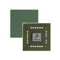
MPC8544VTALF Freescale Semiconductor, MPC8544VTALF Datasheet - Page 110

MPC8544VTALF
Manufacturer Part Number
MPC8544VTALF
Description
MPU POWERQUICC III 783-PBGA
Manufacturer
Freescale Semiconductor
Datasheets
1.MPC8544VTALF.pdf
(117 pages)
2.MPC8544VTALF.pdf
(2 pages)
3.MPC8544VTALF.pdf
(1340 pages)
Specifications of MPC8544VTALF
Processor Type
MPC85xx PowerQUICC III 32-Bit
Speed
667MHz
Voltage
1V
Mounting Type
Surface Mount
Package / Case
783-FCPBGA
Processor Series
MPC85xx
Core
e500
Data Bus Width
32 bit
Maximum Clock Frequency
667 MHz
Maximum Operating Temperature
+ 105 C
Mounting Style
SMD/SMT
Data Ram Size
32 KB
I/o Voltage
1.8 V, 3.3 V
Interface Type
I2C, HSSI, DUART
Minimum Operating Temperature
0 C
Lead Free Status / RoHS Status
Lead free / RoHS Compliant
Features
-
Lead Free Status / Rohs Status
Lead free / RoHS Compliant
Available stocks
Company
Part Number
Manufacturer
Quantity
Price
Company:
Part Number:
MPC8544VTALF
Manufacturer:
Freescale Semiconductor
Quantity:
10 000
Company:
Part Number:
MPC8544VTALFA
Manufacturer:
Freescale Semiconductor
Quantity:
10 000
- Current page: 110 of 1340
- Download datasheet (12Mb)
Overview
1.3.2
The MPC8544E contains an internal 256-Kbyte memory array that can be configured as memory-mapped
SRAM or as a look-aside L2 cache. The array can also be divided into two arrays, one of which may be
used as cache and the other as SRAM.
The memory controller for this array connects to the core complex bus (CCB) and communicates via
128-bit read and write buses to the e500 core and theMPC8544E system logic.
The on-chip memory unit contains:
1-12
•
•
•
— Instruction L1 MMU
— Unified L2 MMU
— Software reload for TLBs
— Support for as much as 4 Gbytes (2
— Support for as much as 64 Gbytes (2
— Support for big-endian and true little-endian memory on a per-page basis
Power management
— Dynamic power management on the core minimizes power consumption of functional units,
— Core power-saving modes: core-halted and core-stopped
— NAP, DOZE, and SLEEP bits in HID0 that can be used to assert nap, doze, and sleep core
Testability
— LSSD scan design
— JTAG interface
— ESP support
256 Kbytes of on-chip memory
— L2 cache partitioning is configurable
— SRAM operation is byte-accessible.
— Data ECC on 64-bit boundaries (single-error correction, double-error detection)
– 64-entry, four-way set-associative TLB for 4-Kbyte pages
– Four-entry, four-way set-associative TLB for 4-Kbyte pages
– 16-entry, fully-associative TLB array for variable-sized pages
– 512-entry, four-way set-associative TLB for 4-Kbyte pages
such as execution units, caches, and MMUs, when they are idle.
output signals to initiate power-saving modes at the integrated device level.
– Can act as a 256-Kbyte L2 cache
– Array can be partitioned into either L2 cache or memory mapped SRAM on a 1-, 2-, 4-, or
– Stashing of I/O data into the L2 array is supported, but can be limited to a 1-, 2-, or 4-way
On-Chip Memory Unit
MPC8544E PowerQUICC III Integrated Host Processor Family Reference Manual, Rev. 1
– 256-Kbyte array organized as 1024 eight-way sets of 32-byte cache lines
8-way basis
basis
32
36
) of virtual memory
) of physical memory
Freescale Semiconductor
Related parts for MPC8544VTALF
Image
Part Number
Description
Manufacturer
Datasheet
Request
R
Part Number:
Description:
Manufacturer:
Freescale Semiconductor, Inc
Datasheet:
Part Number:
Description:
Manufacturer:
Freescale Semiconductor, Inc
Datasheet:
Part Number:
Description:
Manufacturer:
Freescale Semiconductor, Inc
Datasheet:
Part Number:
Description:
Manufacturer:
Freescale Semiconductor, Inc
Datasheet:
Part Number:
Description:
Manufacturer:
Freescale Semiconductor, Inc
Datasheet:
Part Number:
Description:
Manufacturer:
Freescale Semiconductor, Inc
Datasheet:
Part Number:
Description:
Manufacturer:
Freescale Semiconductor, Inc
Datasheet:
Part Number:
Description:
Manufacturer:
Freescale Semiconductor, Inc
Datasheet:
Part Number:
Description:
Manufacturer:
Freescale Semiconductor, Inc
Datasheet:
Part Number:
Description:
Manufacturer:
Freescale Semiconductor, Inc
Datasheet:
Part Number:
Description:
Manufacturer:
Freescale Semiconductor, Inc
Datasheet:
Part Number:
Description:
Manufacturer:
Freescale Semiconductor, Inc
Datasheet:
Part Number:
Description:
Manufacturer:
Freescale Semiconductor, Inc
Datasheet:
Part Number:
Description:
Manufacturer:
Freescale Semiconductor, Inc
Datasheet:
Part Number:
Description:
Manufacturer:
Freescale Semiconductor, Inc
Datasheet:


