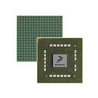
MPC8544VTALF Freescale Semiconductor, MPC8544VTALF Datasheet - Page 331

MPC8544VTALF
Manufacturer Part Number
MPC8544VTALF
Description
MPU POWERQUICC III 783-PBGA
Manufacturer
Freescale Semiconductor
Datasheets
1.MPC8544VTALF.pdf
(117 pages)
2.MPC8544VTALF.pdf
(2 pages)
3.MPC8544VTALF.pdf
(1340 pages)
Specifications of MPC8544VTALF
Processor Type
MPC85xx PowerQUICC III 32-Bit
Speed
667MHz
Voltage
1V
Mounting Type
Surface Mount
Package / Case
783-FCPBGA
Processor Series
MPC85xx
Core
e500
Data Bus Width
32 bit
Maximum Clock Frequency
667 MHz
Maximum Operating Temperature
+ 105 C
Mounting Style
SMD/SMT
Data Ram Size
32 KB
I/o Voltage
1.8 V, 3.3 V
Interface Type
I2C, HSSI, DUART
Minimum Operating Temperature
0 C
Lead Free Status / RoHS Status
Lead free / RoHS Compliant
Features
-
Lead Free Status / Rohs Status
Lead free / RoHS Compliant
Available stocks
Company
Part Number
Manufacturer
Quantity
Price
Company:
Part Number:
MPC8544VTALF
Manufacturer:
Freescale Semiconductor
Quantity:
10 000
Company:
Part Number:
MPC8544VTALFA
Manufacturer:
Freescale Semiconductor
Quantity:
10 000
- Current page: 331 of 1340
- Download datasheet (12Mb)
Freescale Semiconductor
MBA[2:0]
MA[15:0]
Signal
MCAS
MRAS
Table 9-3. Memory Interface Signals—Detailed Signal Descriptions (continued)
MPC8544E PowerQUICC III Integrated Host Processor Family Reference Manual, Rev. 1
I/O
O
O
O
O
Address bus. Memory controller outputs for the address to the DRAM. MA[15:0] carry 16 of the address
bits for the DDR memory interface corresponding to the row and column address bits. MA0 is the lsb of
the address output from the memory controller.
Logical bank address. Outputs that drive the logical (or internal) bank address pins of the SDRAM. Each
SDRAM supports four or eight addressable logical sub-banks. Bit zero of the memory controller’s output
bank address must be connected to bit zero of the SDRAM’s input bank address. MBA0, the
least-significant bit of the three bank address signals, is asserted during the mode register set command
to specify the extended mode register.
Column address strobe. Active-low SDRAM address multiplexing signal. MCAS is asserted for read or
write transactions and for mode register set, refresh, and precharge commands.
Row address strobe. Active-low SDRAM address multiplexing signal. Asserted for activate commands.
In addition; used for mode register set commands and refresh commands.
Meaning
Meaning
Meaning
Meaning
Timing Assertion/Negation—The address is always driven when the memory controller is enabled.
Timing Assertion/Negation—Same timing as MA n
Timing Assertion/Negation—Assertion and negation timing is directed by the values described in
Timing Assertion/Negation—Assertion and negation timing is directed by the values described in
State
State
State
State
Asserted/Negated—Represents the address driven by the DDR memory controller. Contains
High impedance—When the memory controller is disabled
Asserted/Negated—Selects the DDR SDRAM logical (or internal) bank to be activated during
High impedance—Same timing as MA n
Asserted—Indicates that a valid SDRAM column address is on the address bus for read and
Negated—The column address is not guaranteed to be valid.
High impedance—MCAS is always driven unless the memory controller is disabled.
Asserted—Indicates that a valid SDRAM row address is on the address bus for read and
Negated—The row address is not guaranteed to be valid.
High impedance—MRAS is always driven unless the memory controller is disabled.
different portions of the address depending on the memory size and the DRAM
command being issued by the memory controller. See
complete description of the mapping of these signals.
It is valid when a transaction is driven to DRAM (when MCS n is active).
the row address phase and selects the SDRAM internal bank for the read or write
operation during the column address phase of the memory access.
Table 9-41Table 9-42
write transactions. See
for various other SDRAM commands.
Section 9.4.1.4, “DDR SDRAM Timing Configuration 0 (TIMING_CFG_0),”
Section 9.4.1.5, “DDR SDRAM Timing Configuration 1 (TIMING_CFG_1),”
Section 9.4.1.6, “DDR SDRAM Timing Configuration 2
Section 9.4.1.3, “DDR SDRAM Timing Configuration 3 (TIMING_CFG_3).”
describes the mapping of these signals in all cases.
Table 9-46
Table 9-46
Description
for more information on the states required on MCAS
for more information on the states required on MRAS
Table 9-41Table 9-42
(TIMING_CFG_2),” and
(TIMING_CFG_2),” and
DDR Memory Controller
for a
9-7
Related parts for MPC8544VTALF
Image
Part Number
Description
Manufacturer
Datasheet
Request
R
Part Number:
Description:
Manufacturer:
Freescale Semiconductor, Inc
Datasheet:
Part Number:
Description:
Manufacturer:
Freescale Semiconductor, Inc
Datasheet:
Part Number:
Description:
Manufacturer:
Freescale Semiconductor, Inc
Datasheet:
Part Number:
Description:
Manufacturer:
Freescale Semiconductor, Inc
Datasheet:
Part Number:
Description:
Manufacturer:
Freescale Semiconductor, Inc
Datasheet:
Part Number:
Description:
Manufacturer:
Freescale Semiconductor, Inc
Datasheet:
Part Number:
Description:
Manufacturer:
Freescale Semiconductor, Inc
Datasheet:
Part Number:
Description:
Manufacturer:
Freescale Semiconductor, Inc
Datasheet:
Part Number:
Description:
Manufacturer:
Freescale Semiconductor, Inc
Datasheet:
Part Number:
Description:
Manufacturer:
Freescale Semiconductor, Inc
Datasheet:
Part Number:
Description:
Manufacturer:
Freescale Semiconductor, Inc
Datasheet:
Part Number:
Description:
Manufacturer:
Freescale Semiconductor, Inc
Datasheet:
Part Number:
Description:
Manufacturer:
Freescale Semiconductor, Inc
Datasheet:
Part Number:
Description:
Manufacturer:
Freescale Semiconductor, Inc
Datasheet:
Part Number:
Description:
Manufacturer:
Freescale Semiconductor, Inc
Datasheet:


