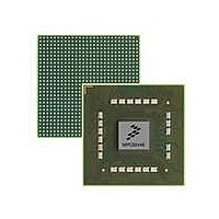
MPC8544VTALF Freescale Semiconductor, MPC8544VTALF Datasheet - Page 161

MPC8544VTALF
Manufacturer Part Number
MPC8544VTALF
Description
MPU POWERQUICC III 783-PBGA
Manufacturer
Freescale Semiconductor
Datasheets
1.MPC8544VTALF.pdf
(117 pages)
2.MPC8544VTALF.pdf
(2 pages)
3.MPC8544VTALF.pdf
(1340 pages)
Specifications of MPC8544VTALF
Processor Type
MPC85xx PowerQUICC III 32-Bit
Speed
667MHz
Voltage
1V
Mounting Type
Surface Mount
Package / Case
783-FCPBGA
Processor Series
MPC85xx
Core
e500
Data Bus Width
32 bit
Maximum Clock Frequency
667 MHz
Maximum Operating Temperature
+ 105 C
Mounting Style
SMD/SMT
Data Ram Size
32 KB
I/o Voltage
1.8 V, 3.3 V
Interface Type
I2C, HSSI, DUART
Minimum Operating Temperature
0 C
Lead Free Status / RoHS Status
Lead free / RoHS Compliant
Features
-
Lead Free Status / Rohs Status
Lead free / RoHS Compliant
Available stocks
Company
Part Number
Manufacturer
Quantity
Price
Company:
Part Number:
MPC8544VTALF
Manufacturer:
Freescale Semiconductor
Quantity:
10 000
Company:
Part Number:
MPC8544VTALFA
Manufacturer:
Freescale Semiconductor
Quantity:
10 000
- Current page: 161 of 1340
- Download datasheet (12Mb)
4.2.2
Table 4-3
to blocks within the MPC8544E, and although some of their functionality is described in
“Clocking,” they are defined in detail in their respective chapters.
Note that there is also a CLK_OUT signal in the MPC8544E; the signal driven on the CLK_OUT pin is
selectable and described in
SYSCLK
Freescale Semiconductor
Signal I/O
RTC
I System clock/PCI clock (SYSCLK/PCI_CLK). SYSCLK is the primary clock input to the MPC8544E. It is the clock
I Real time clock. May be used (optionally) to clock the time base of the e500 core. The RTC timing specifications
describes the overall clock signals of the MPC8544E. Note that some clock signals are specific
source for the e500 core and for all devices and interfaces that operate synchronously with the core. It is multiplied
up with a phased-lock loop (PLL) to create the core complex bus (CCB) clock (also called the platform clock), which
is used by virtually all of the synchronous system logic, including the L2 cache, the DDR SDRAM and local bus
memory controllers, and other internal blocks such as the DMA and interrupt controllers. The CCB clock, in turn,
feeds the PLL in the e500 core and the PLL that creates the local bus memory clocks.
When the PCI interface is used, SYSCLK also functions as the PCI_CLK signal. Note that this is true whether the
MPC8544E is in agent or host mode. The MPC8544E does not provide a separate PCI_CLK output in host mode.
are given in the MPC8544E Integrated Processor Hardware Specifications , but the maximum frequency should be
less than one-quarter of the CCB frequency. See
(optionally) to clock the global timers in the programmable interrupt controller (PIC).
Clock Signals
MPC8544E PowerQUICC III Integrated Host Processor Family Reference Manual, Rev. 1
Timing Assertion/Negation—See the MPC8544E Integrated Processor Hardware Specifications for specific
Timing Assertion/Negation—See the MPC8544E Integrated Processor Hardware Specifications for specific
Table 4-3. Clock Signals—Detailed Signal Descriptions
timing information for this signal.
timing information for this signal.
Section 19.4.1.23, “Clock Out Control Register (CLKOCR).”
Section 4.4.4.4, “Real Time
Description
Clock.” This signal can also be used
Reset, Clocking, and Initialization
Section 4.4.4,
4-3
Related parts for MPC8544VTALF
Image
Part Number
Description
Manufacturer
Datasheet
Request
R
Part Number:
Description:
Manufacturer:
Freescale Semiconductor, Inc
Datasheet:
Part Number:
Description:
Manufacturer:
Freescale Semiconductor, Inc
Datasheet:
Part Number:
Description:
Manufacturer:
Freescale Semiconductor, Inc
Datasheet:
Part Number:
Description:
Manufacturer:
Freescale Semiconductor, Inc
Datasheet:
Part Number:
Description:
Manufacturer:
Freescale Semiconductor, Inc
Datasheet:
Part Number:
Description:
Manufacturer:
Freescale Semiconductor, Inc
Datasheet:
Part Number:
Description:
Manufacturer:
Freescale Semiconductor, Inc
Datasheet:
Part Number:
Description:
Manufacturer:
Freescale Semiconductor, Inc
Datasheet:
Part Number:
Description:
Manufacturer:
Freescale Semiconductor, Inc
Datasheet:
Part Number:
Description:
Manufacturer:
Freescale Semiconductor, Inc
Datasheet:
Part Number:
Description:
Manufacturer:
Freescale Semiconductor, Inc
Datasheet:
Part Number:
Description:
Manufacturer:
Freescale Semiconductor, Inc
Datasheet:
Part Number:
Description:
Manufacturer:
Freescale Semiconductor, Inc
Datasheet:
Part Number:
Description:
Manufacturer:
Freescale Semiconductor, Inc
Datasheet:
Part Number:
Description:
Manufacturer:
Freescale Semiconductor, Inc
Datasheet:


