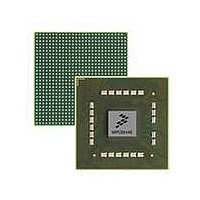
MPC8544VTALF Freescale Semiconductor, MPC8544VTALF Datasheet - Page 1032

MPC8544VTALF
Manufacturer Part Number
MPC8544VTALF
Description
MPU POWERQUICC III 783-PBGA
Manufacturer
Freescale Semiconductor
Datasheets
1.MPC8544VTALF.pdf
(117 pages)
2.MPC8544VTALF.pdf
(2 pages)
3.MPC8544VTALF.pdf
(1340 pages)
Specifications of MPC8544VTALF
Processor Type
MPC85xx PowerQUICC III 32-Bit
Speed
667MHz
Voltage
1V
Mounting Type
Surface Mount
Package / Case
783-FCPBGA
Processor Series
MPC85xx
Core
e500
Data Bus Width
32 bit
Maximum Clock Frequency
667 MHz
Maximum Operating Temperature
+ 105 C
Mounting Style
SMD/SMT
Data Ram Size
32 KB
I/o Voltage
1.8 V, 3.3 V
Interface Type
I2C, HSSI, DUART
Minimum Operating Temperature
0 C
Lead Free Status / RoHS Status
Lead free / RoHS Compliant
Features
-
Lead Free Status / Rohs Status
Lead free / RoHS Compliant
Available stocks
Company
Part Number
Manufacturer
Quantity
Price
Company:
Part Number:
MPC8544VTALF
Manufacturer:
Freescale Semiconductor
Quantity:
10 000
Company:
Part Number:
MPC8544VTALFA
Manufacturer:
Freescale Semiconductor
Quantity:
10 000
- Current page: 1032 of 1340
- Download datasheet (12Mb)
PCI Bus Interface
PCI_AD[1:0] = 01 or PCI_AD[1:0] = 0b11 during the address phase of a local memory access. See
Section 17.4.2.8.2, “Target-Initiated Termination,”
For linear incrementing mode, the memory address is encoded/decoded using PCI_AD[31:2]. Thereafter,
the address is incremented by 4 bytes after each data phase completes until the transaction is terminated
or completed (a 4-byte data width per data phase is implied). Note that the two low-order bits on the
address bus are included in all parity calculations.
For cache wrap mode (PCI_AD[1:0] = 0b10) reads, the critical memory address is decoded using
PCI_AD[31:2]. The address is incremented by 4 bytes after each data phase completes until the end of the
cache line is reached. For cache-wrap reads, the address wraps to the beginning of the current cache line
and continues incrementing until the entire cache line (32 bytes) is read. The PCI controller does not
support cache-wrap write operations and executes a target disconnect after the data phase for the end of
the cache line completes for writes with PCI_AD[1:0] = 0b10. That is, the PCI controller does not wrap
back to the beginning of the cache line. Note that the two low-order bits on the address bus are included
in all parity calculations.
17.4.2.3.2
For PCI I/O accesses, 32 address signals (PCI_AD[31:0]) are used to provide a byte address. After a target
has claimed an I/O access, it must determine if it can complete the entire access as indicated by the byte
enable signals. If all the selected bytes are not in the address range of the target, the entire access cannot
complete. In this case, the target does not transfer any data and terminates the transaction with a
target-abort error. See
17.4.2.3.3
PCI supports two types of configuration accesses that use different formats for the PCI_AD[31:0] signals
during the address phase. The two low-order bits of the address indicate the format used for the
configuration address phase—type 0 (PCI_AD[1:0] = 0b00) or type 1 (PCI_AD[1:0] = 0b01). Both
address formats identify a specific device and a specific configuration register for that device. See
Section 17.4.2.11, “Configuration Cycles,”
17.4.2.4
The PCI_DEVSEL signal is driven by the target of the current transaction. PCI_DEVSEL indicates to the
other devices on the PCI bus that the target has decoded the address and claimed the transaction.
17-48
Device Selection
MPC8544E PowerQUICC III Integrated Host Processor Family Reference Manual, Rev. 1
I/O Space Addressing
Configuration Space Addressing
00
01
10
11
Section 17.4.2.8.2, “Target-Initiated Termination,”
PCI_AD[1:0]
Linear
Reserved
Cache Wrap
Reserved
Table 17-48. Supported Combinations of PCI_AD[1:0]
Read
for descriptions of the two formats.
TD
TD
√
√
Target
for more information on target disconnect conditions.
Write
TD
TD
TD
√
Read
—
—
—
√
Initiator
for more information.
Write
—
—
—
√
Freescale Semiconductor
Related parts for MPC8544VTALF
Image
Part Number
Description
Manufacturer
Datasheet
Request
R
Part Number:
Description:
Manufacturer:
Freescale Semiconductor, Inc
Datasheet:
Part Number:
Description:
Manufacturer:
Freescale Semiconductor, Inc
Datasheet:
Part Number:
Description:
Manufacturer:
Freescale Semiconductor, Inc
Datasheet:
Part Number:
Description:
Manufacturer:
Freescale Semiconductor, Inc
Datasheet:
Part Number:
Description:
Manufacturer:
Freescale Semiconductor, Inc
Datasheet:
Part Number:
Description:
Manufacturer:
Freescale Semiconductor, Inc
Datasheet:
Part Number:
Description:
Manufacturer:
Freescale Semiconductor, Inc
Datasheet:
Part Number:
Description:
Manufacturer:
Freescale Semiconductor, Inc
Datasheet:
Part Number:
Description:
Manufacturer:
Freescale Semiconductor, Inc
Datasheet:
Part Number:
Description:
Manufacturer:
Freescale Semiconductor, Inc
Datasheet:
Part Number:
Description:
Manufacturer:
Freescale Semiconductor, Inc
Datasheet:
Part Number:
Description:
Manufacturer:
Freescale Semiconductor, Inc
Datasheet:
Part Number:
Description:
Manufacturer:
Freescale Semiconductor, Inc
Datasheet:
Part Number:
Description:
Manufacturer:
Freescale Semiconductor, Inc
Datasheet:
Part Number:
Description:
Manufacturer:
Freescale Semiconductor, Inc
Datasheet:


