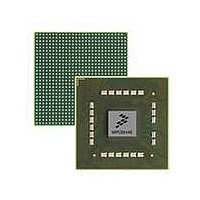
MPC8544VTALF Freescale Semiconductor, MPC8544VTALF Datasheet - Page 1162

MPC8544VTALF
Manufacturer Part Number
MPC8544VTALF
Description
MPU POWERQUICC III 783-PBGA
Manufacturer
Freescale Semiconductor
Datasheets
1.MPC8544VTALF.pdf
(117 pages)
2.MPC8544VTALF.pdf
(2 pages)
3.MPC8544VTALF.pdf
(1340 pages)
Specifications of MPC8544VTALF
Processor Type
MPC85xx PowerQUICC III 32-Bit
Speed
667MHz
Voltage
1V
Mounting Type
Surface Mount
Package / Case
783-FCPBGA
Processor Series
MPC85xx
Core
e500
Data Bus Width
32 bit
Maximum Clock Frequency
667 MHz
Maximum Operating Temperature
+ 105 C
Mounting Style
SMD/SMT
Data Ram Size
32 KB
I/o Voltage
1.8 V, 3.3 V
Interface Type
I2C, HSSI, DUART
Minimum Operating Temperature
0 C
Lead Free Status / RoHS Status
Lead free / RoHS Compliant
Features
-
Lead Free Status / Rohs Status
Lead free / RoHS Compliant
Available stocks
Company
Part Number
Manufacturer
Quantity
Price
Company:
Part Number:
MPC8544VTALF
Manufacturer:
Freescale Semiconductor
Quantity:
10 000
Company:
Part Number:
MPC8544VTALFA
Manufacturer:
Freescale Semiconductor
Quantity:
10 000
- Current page: 1162 of 1340
- Download datasheet (12Mb)
PCI Express Interface Controller
18.4.4
All device power states are supported with the exception of D3cold with Vaux. In addition, all link power
states are supported with the exception of L2 states. Only L0s ASPM mode is supported if enabled by
configuring the Link Control register’s bits 1–0 in configuration space. Note that there is no power saving
in the controller when the device is put into a non-D0 state. The only power saving is the I/O drivers when
the controller is put into a non-L0 link state.
18.4.4.1
The L2/L3 Ready link state is entered after the EP device is put into a D3hot state followed by a
PME_Turn_Off/PME_TO_Ack message handshake protocol. Exiting this state requires a POR reset or a
WAKE signal from the EP device. The PCI Express controller (in EP mode) does not support the
generation of beacon; therefore, as an alternative, the device can use one of the GPIO signals as an enable
to an external tristate buffer to generate a WAKE signal, as shown in
18-108
Component
D-State
D3cold
D3hot
D0
D1
D2
Power Management
L2/L3 Ready Link State
MPC8544E PowerQUICC III Integrated Host Processor Family Reference Manual, Rev. 1
L0, L0s, L1, L2/L3
Interconnect
Permissible
L0, L0s, L1
L0, L0s, L1
CPLD (Memory Read Completion, IO Read
L0, L0s
CPLH (Memory Read Completion, IO R/W
Ready
State
L3
Completion, Cfg Read Completion)
Completion, Cfg R/W Completion)
Table 18-123. Power Management State Supported
In full operation.
All outbound traffics are stalled. All inbound traffics will be thrown away. The only
exceptions are PME messages and configuration transactions. If the device is in RC
mode, it is permissible to send a PM_Turn_Off message via the PEX Power
Management Command register.
All outbound traffics are stalled. All inbound traffics will be thrown away. The only
exceptions are PME messages and configuration transactions. If the device is in RC
mode, it is permissible to send a PM_Turn_Off message via the PEX Power
Management Command register.
All outbound traffics are stalled. All inbound traffics will be thrown away. The only
exceptions are PME messages and configuration transactions. If the device is in RC
mode, it is permissible to send a PM_Turn_Off message via the PEX Power
Management Command register. Note that if a transition of D3hot->D0 occurs, a reset
is performed to the controller’s configuration space. In addition, link training will restart.
Completely off.
Credit Type
Table 18-122. Initial credit advertisement
Initial Credit Advertisement
Action
Figure
Infinite
Infinite
18-130.
Freescale Semiconductor
Related parts for MPC8544VTALF
Image
Part Number
Description
Manufacturer
Datasheet
Request
R
Part Number:
Description:
Manufacturer:
Freescale Semiconductor, Inc
Datasheet:
Part Number:
Description:
Manufacturer:
Freescale Semiconductor, Inc
Datasheet:
Part Number:
Description:
Manufacturer:
Freescale Semiconductor, Inc
Datasheet:
Part Number:
Description:
Manufacturer:
Freescale Semiconductor, Inc
Datasheet:
Part Number:
Description:
Manufacturer:
Freescale Semiconductor, Inc
Datasheet:
Part Number:
Description:
Manufacturer:
Freescale Semiconductor, Inc
Datasheet:
Part Number:
Description:
Manufacturer:
Freescale Semiconductor, Inc
Datasheet:
Part Number:
Description:
Manufacturer:
Freescale Semiconductor, Inc
Datasheet:
Part Number:
Description:
Manufacturer:
Freescale Semiconductor, Inc
Datasheet:
Part Number:
Description:
Manufacturer:
Freescale Semiconductor, Inc
Datasheet:
Part Number:
Description:
Manufacturer:
Freescale Semiconductor, Inc
Datasheet:
Part Number:
Description:
Manufacturer:
Freescale Semiconductor, Inc
Datasheet:
Part Number:
Description:
Manufacturer:
Freescale Semiconductor, Inc
Datasheet:
Part Number:
Description:
Manufacturer:
Freescale Semiconductor, Inc
Datasheet:
Part Number:
Description:
Manufacturer:
Freescale Semiconductor, Inc
Datasheet:


