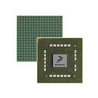
MPC8544VTALF Freescale Semiconductor, MPC8544VTALF Datasheet - Page 464

MPC8544VTALF
Manufacturer Part Number
MPC8544VTALF
Description
MPU POWERQUICC III 783-PBGA
Manufacturer
Freescale Semiconductor
Datasheets
1.MPC8544VTALF.pdf
(117 pages)
2.MPC8544VTALF.pdf
(2 pages)
3.MPC8544VTALF.pdf
(1340 pages)
Specifications of MPC8544VTALF
Processor Type
MPC85xx PowerQUICC III 32-Bit
Speed
667MHz
Voltage
1V
Mounting Type
Surface Mount
Package / Case
783-FCPBGA
Processor Series
MPC85xx
Core
e500
Data Bus Width
32 bit
Maximum Clock Frequency
667 MHz
Maximum Operating Temperature
+ 105 C
Mounting Style
SMD/SMT
Data Ram Size
32 KB
I/o Voltage
1.8 V, 3.3 V
Interface Type
I2C, HSSI, DUART
Minimum Operating Temperature
0 C
Lead Free Status / RoHS Status
Lead free / RoHS Compliant
Features
-
Lead Free Status / Rohs Status
Lead free / RoHS Compliant
Available stocks
Company
Part Number
Manufacturer
Quantity
Price
Company:
Part Number:
MPC8544VTALF
Manufacturer:
Freescale Semiconductor
Quantity:
10 000
Company:
Part Number:
MPC8544VTALFA
Manufacturer:
Freescale Semiconductor
Quantity:
10 000
- Current page: 464 of 1340
- Download datasheet (12Mb)
I
11.3.1.5
The I2C data register is shown in
Table 11-8
11-10
2
C Interfaces
Bits
Bits
0–7
6
7
Name
RXAK Received acknowledge. The value of SDA during the reception of acknowledge bit of a bus cycle. If the
Name
DATA
MIF
shows the bit descriptions for I2CDR.
Offset I
Reset
MPC8544E PowerQUICC III Integrated Host Processor Family Reference Manual, Rev. 1
I
Module interrupt. The MIF bit is set when an interrupt is pending, causing a processor interrupt request
(provided I2CCR[MIEN] is set). The interrupts for I
sourced by the dual I
0 No interrupt is pending. Can be cleared only by software.
1 Interrupt is pending. MIF is set when one of the following events occurs:
received acknowledge bit (RXAK) is low, it indicates that an acknowledge signal has been received after the
completion of eight bits of data transmission on the bus. If RXAK is high, it means no acknowledge signal has
been detected at the 9th clock.
0 Acknowledge received
1 No acknowledge received
Transmission starts when an address and the R/W bit are written to the data register and the I
performs as the master. A data transfer is initiated when data is written to the I2CDR. The most significant bit
is sent first in both cases. In master receive mode, reading the data register allows the read to occur, but also
allows the I
is available after it is addressed. Note that the very first read is always a dummy read.
2
W
R
C Data Register (I2CDR)
•One byte of data is transferred (set at the falling edge of the 9th clock).
•The value in I2CADR matches with the calling address in slave-receive mode.
•Arbitration is lost.
I
2
2
C1: 0x010
C2: 0x110
0
2
C module to receive the next byte of data on the I
Table 11-7. I2CSR Field Descriptions (continued)
2
C controller.
Figure
Figure 11-6. I
Table 11-8. I2CDR Field Descriptions
11-6.
2
C Data Register (I2CDR)
All zeros
DATA
Description
Description
2
C1 and I
2
C2 are combined into one interrupt, which is
2
C interface. In slave mode, the same function
Access: Read/Write
Freescale Semiconductor
7
2
C interface
Related parts for MPC8544VTALF
Image
Part Number
Description
Manufacturer
Datasheet
Request
R
Part Number:
Description:
Manufacturer:
Freescale Semiconductor, Inc
Datasheet:
Part Number:
Description:
Manufacturer:
Freescale Semiconductor, Inc
Datasheet:
Part Number:
Description:
Manufacturer:
Freescale Semiconductor, Inc
Datasheet:
Part Number:
Description:
Manufacturer:
Freescale Semiconductor, Inc
Datasheet:
Part Number:
Description:
Manufacturer:
Freescale Semiconductor, Inc
Datasheet:
Part Number:
Description:
Manufacturer:
Freescale Semiconductor, Inc
Datasheet:
Part Number:
Description:
Manufacturer:
Freescale Semiconductor, Inc
Datasheet:
Part Number:
Description:
Manufacturer:
Freescale Semiconductor, Inc
Datasheet:
Part Number:
Description:
Manufacturer:
Freescale Semiconductor, Inc
Datasheet:
Part Number:
Description:
Manufacturer:
Freescale Semiconductor, Inc
Datasheet:
Part Number:
Description:
Manufacturer:
Freescale Semiconductor, Inc
Datasheet:
Part Number:
Description:
Manufacturer:
Freescale Semiconductor, Inc
Datasheet:
Part Number:
Description:
Manufacturer:
Freescale Semiconductor, Inc
Datasheet:
Part Number:
Description:
Manufacturer:
Freescale Semiconductor, Inc
Datasheet:
Part Number:
Description:
Manufacturer:
Freescale Semiconductor, Inc
Datasheet:


