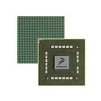
MPC8544VTALF Freescale Semiconductor, MPC8544VTALF Datasheet - Page 1147

MPC8544VTALF
Manufacturer Part Number
MPC8544VTALF
Description
MPU POWERQUICC III 783-PBGA
Manufacturer
Freescale Semiconductor
Datasheets
1.MPC8544VTALF.pdf
(117 pages)
2.MPC8544VTALF.pdf
(2 pages)
3.MPC8544VTALF.pdf
(1340 pages)
Specifications of MPC8544VTALF
Processor Type
MPC85xx PowerQUICC III 32-Bit
Speed
667MHz
Voltage
1V
Mounting Type
Surface Mount
Package / Case
783-FCPBGA
Processor Series
MPC85xx
Core
e500
Data Bus Width
32 bit
Maximum Clock Frequency
667 MHz
Maximum Operating Temperature
+ 105 C
Mounting Style
SMD/SMT
Data Ram Size
32 KB
I/o Voltage
1.8 V, 3.3 V
Interface Type
I2C, HSSI, DUART
Minimum Operating Temperature
0 C
Lead Free Status / RoHS Status
Lead free / RoHS Compliant
Features
-
Lead Free Status / Rohs Status
Lead free / RoHS Compliant
Available stocks
Company
Part Number
Manufacturer
Quantity
Price
Company:
Part Number:
MPC8544VTALF
Manufacturer:
Freescale Semiconductor
Quantity:
10 000
Company:
Part Number:
MPC8544VTALFA
Manufacturer:
Freescale Semiconductor
Quantity:
10 000
- Current page: 1147 of 1340
- Download datasheet (12Mb)
The fields of the PCI Express power management timer register are described in
18.3.10.16 PCI Express PME Time-Out Register (EP-Mode Only)—0x454
The PCI Express PME time-out register, shown in
that the controller uses before re-sending a PME message to the host. If PME is requested by a function
and the host does not clear the associated PME_STAT bit even after this time-out has expired, the PME
message is sent again to the host by the PCI Express controller. This register is supported only for EP
mode.
The fields of the PCI Express PME time-out register are described in
Freescale Semiconductor
31–24
23–12 L1_WAIT_PERIOD Wait period (in PCI Express controller core clock cycles) before entering L1 power state after all
31–26
11–0
25–0
Offset 0x454 (EP-mode only)
Bits
Reset 0
Bits
W
R
31
PME_TIMEOUT
L0s_TIME_IN
0
Name
Name
MPC8544E PowerQUICC III Integrated Host Processor Family Reference Manual, Rev. 1
0
—
—
—
Figure 18-117. PCI Express PME Time-Out Register (PEX_PME_TIMEOUT)
0
0
26 25
0
Reserved
functions are in a non-D0 power state. The value is calculated as:
The time value must be less than 2 µsec; the default value (0x14D) is 1 µsec for the default clock
frequency of 333 MHz.
Time in value (in PCI Express controller core clock cycles) for entering L0s power state. The
value is calculated as:
The maximum time value is 7 µsec; the default value (0x7CE) is 6 µsec for the default clock
frequency of 333 MHz.
Reserved
The PME time-out value specifies the interval before PME messages are resent by the controller,
provided the PME_STAT bit in the PCI Express power management status and control register
(offset 0x48) is not cleared by the host. The value for PME_TIMEOUT is specified in terms of
PCI Express controller core clock cycles. The value is calculated as:
The minimum time value is 100 msec; the default value (0x1FC1E20) is 100 msec for the default
clock frequency of 333 MHz.
Table 18-112. PEX_PME_TIMEOUT Field Descriptions
0
Time (in µsec) × PCI Express controller core clock frequency (in MHz)
Time (in µsec) × PCI Express controller core clock frequency (in MHz)
Time (in µsec) × PCI Express controller core clock frequency (in MHz)
Table 18-111. PEX_PM_TIMER Field Descriptions
1
1
1
1
1
1
1
0
Figure
0
0
PME_TIMEOUT
18-117, is used to program the time-out value
Description
Description
0
0
1
1
Table
1
1
18-111.
0
PCI Express Interface Controller
0
Table
0
1
18-111.
0
Access: Mixed
0
0
0
18-93
0
0
Related parts for MPC8544VTALF
Image
Part Number
Description
Manufacturer
Datasheet
Request
R
Part Number:
Description:
Manufacturer:
Freescale Semiconductor, Inc
Datasheet:
Part Number:
Description:
Manufacturer:
Freescale Semiconductor, Inc
Datasheet:
Part Number:
Description:
Manufacturer:
Freescale Semiconductor, Inc
Datasheet:
Part Number:
Description:
Manufacturer:
Freescale Semiconductor, Inc
Datasheet:
Part Number:
Description:
Manufacturer:
Freescale Semiconductor, Inc
Datasheet:
Part Number:
Description:
Manufacturer:
Freescale Semiconductor, Inc
Datasheet:
Part Number:
Description:
Manufacturer:
Freescale Semiconductor, Inc
Datasheet:
Part Number:
Description:
Manufacturer:
Freescale Semiconductor, Inc
Datasheet:
Part Number:
Description:
Manufacturer:
Freescale Semiconductor, Inc
Datasheet:
Part Number:
Description:
Manufacturer:
Freescale Semiconductor, Inc
Datasheet:
Part Number:
Description:
Manufacturer:
Freescale Semiconductor, Inc
Datasheet:
Part Number:
Description:
Manufacturer:
Freescale Semiconductor, Inc
Datasheet:
Part Number:
Description:
Manufacturer:
Freescale Semiconductor, Inc
Datasheet:
Part Number:
Description:
Manufacturer:
Freescale Semiconductor, Inc
Datasheet:
Part Number:
Description:
Manufacturer:
Freescale Semiconductor, Inc
Datasheet:


