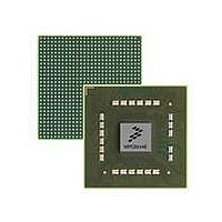
MPC8544VTALF Freescale Semiconductor, MPC8544VTALF Datasheet - Page 641

MPC8544VTALF
Manufacturer Part Number
MPC8544VTALF
Description
MPU POWERQUICC III 783-PBGA
Manufacturer
Freescale Semiconductor
Datasheets
1.MPC8544VTALF.pdf
(117 pages)
2.MPC8544VTALF.pdf
(2 pages)
3.MPC8544VTALF.pdf
(1340 pages)
Specifications of MPC8544VTALF
Processor Type
MPC85xx PowerQUICC III 32-Bit
Speed
667MHz
Voltage
1V
Mounting Type
Surface Mount
Package / Case
783-FCPBGA
Processor Series
MPC85xx
Core
e500
Data Bus Width
32 bit
Maximum Clock Frequency
667 MHz
Maximum Operating Temperature
+ 105 C
Mounting Style
SMD/SMT
Data Ram Size
32 KB
I/o Voltage
1.8 V, 3.3 V
Interface Type
I2C, HSSI, DUART
Minimum Operating Temperature
0 C
Lead Free Status / RoHS Status
Lead free / RoHS Compliant
Features
-
Lead Free Status / Rohs Status
Lead free / RoHS Compliant
Available stocks
Company
Part Number
Manufacturer
Quantity
Price
Company:
Part Number:
MPC8544VTALF
Manufacturer:
Freescale Semiconductor
Quantity:
10 000
Company:
Part Number:
MPC8544VTALFA
Manufacturer:
Freescale Semiconductor
Quantity:
10 000
- Current page: 641 of 1340
- Download datasheet (12Mb)
14.3.1.7
The local bus SDRAM mode register (LSDMR), shown in
pertaining to SDRAM.
Table 14-12
Freescale Semiconductor
11–13
Offset 0x094
Reset
8–10
Bits
2–4
5–7
0
1
W
R
— RFEN
0
BSMA
Name
RFEN
1
OP
—
—
—
describes LSDMR fields.
MPC8544E PowerQUICC III Integrated Host Processor Family Reference Manual, Rev. 1
SDRAM Machine Mode Register (LSDMR)
2
OP
Reserved
Refresh enable. Indicates that the SDRAM requires refresh services.
0 Refresh services are not required.
1 Refresh services are required.
SDRAM operation. Selects the operation that occurs when the SDRAM device is accessed.
Reserved
Bank select multiplexed address line. Selects which address signals serve as the 2-bit bank-select
address for SDRAM. Note that only 4-bank SDRAMs are supported.
000 LA12:LA13
001 LA13:LA14
010 LA14:LA15
011 LA15:LA16
Reserved
4 5
—
Figure 14-10. SDRAM Machine Mode Register (LSDMR)
7
Value
8
000
001
010
011
100
101
110
111
BSMA
Table 14-13. LSDMR Field Descriptions
10 11
Normal operation
Auto refresh
Self refresh
Mode Register write
Precharge bank
Precharge all banks
Activate bank
Read/write without valid data transfer
—
13 14
RFCR
100 LA16:LA17
101 LA17:LA18
110 LA18:LA19
111 LA19:LA20
Meaning
16 17
All zeros
PRETOACT ACTTORW BL
Description
Figure
19
20
14-10, is used to configure operations
Normal operation
Initialization
Power-down mode or debug
Initialization
Debug
Initialization
Debug
Debug
22
23 24 25 26 27 28
—
Use
WRC — BUFCMD
Access: Read/Write
Local Bus Controller
29
30 31
14-21
CL
Related parts for MPC8544VTALF
Image
Part Number
Description
Manufacturer
Datasheet
Request
R
Part Number:
Description:
Manufacturer:
Freescale Semiconductor, Inc
Datasheet:
Part Number:
Description:
Manufacturer:
Freescale Semiconductor, Inc
Datasheet:
Part Number:
Description:
Manufacturer:
Freescale Semiconductor, Inc
Datasheet:
Part Number:
Description:
Manufacturer:
Freescale Semiconductor, Inc
Datasheet:
Part Number:
Description:
Manufacturer:
Freescale Semiconductor, Inc
Datasheet:
Part Number:
Description:
Manufacturer:
Freescale Semiconductor, Inc
Datasheet:
Part Number:
Description:
Manufacturer:
Freescale Semiconductor, Inc
Datasheet:
Part Number:
Description:
Manufacturer:
Freescale Semiconductor, Inc
Datasheet:
Part Number:
Description:
Manufacturer:
Freescale Semiconductor, Inc
Datasheet:
Part Number:
Description:
Manufacturer:
Freescale Semiconductor, Inc
Datasheet:
Part Number:
Description:
Manufacturer:
Freescale Semiconductor, Inc
Datasheet:
Part Number:
Description:
Manufacturer:
Freescale Semiconductor, Inc
Datasheet:
Part Number:
Description:
Manufacturer:
Freescale Semiconductor, Inc
Datasheet:
Part Number:
Description:
Manufacturer:
Freescale Semiconductor, Inc
Datasheet:
Part Number:
Description:
Manufacturer:
Freescale Semiconductor, Inc
Datasheet:


