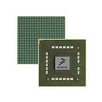
MPC8544VTALF Freescale Semiconductor, MPC8544VTALF Datasheet - Page 663

MPC8544VTALF
Manufacturer Part Number
MPC8544VTALF
Description
MPU POWERQUICC III 783-PBGA
Manufacturer
Freescale Semiconductor
Datasheets
1.MPC8544VTALF.pdf
(117 pages)
2.MPC8544VTALF.pdf
(2 pages)
3.MPC8544VTALF.pdf
(1340 pages)
Specifications of MPC8544VTALF
Processor Type
MPC85xx PowerQUICC III 32-Bit
Speed
667MHz
Voltage
1V
Mounting Type
Surface Mount
Package / Case
783-FCPBGA
Processor Series
MPC85xx
Core
e500
Data Bus Width
32 bit
Maximum Clock Frequency
667 MHz
Maximum Operating Temperature
+ 105 C
Mounting Style
SMD/SMT
Data Ram Size
32 KB
I/o Voltage
1.8 V, 3.3 V
Interface Type
I2C, HSSI, DUART
Minimum Operating Temperature
0 C
Lead Free Status / RoHS Status
Lead free / RoHS Compliant
Features
-
Lead Free Status / Rohs Status
Lead free / RoHS Compliant
Available stocks
Company
Part Number
Manufacturer
Quantity
Price
Company:
Part Number:
MPC8544VTALF
Manufacturer:
Freescale Semiconductor
Quantity:
10 000
Company:
Part Number:
MPC8544VTALFA
Manufacturer:
Freescale Semiconductor
Quantity:
10 000
- Current page: 663 of 1340
- Download datasheet (12Mb)
14.4.2.2.4
The timing of LOE is affected only by TRLX. It always asserts and negates on the rising edge of the bus
clock. LOE asserts either on the rising edge of the bus clock after LCSn is asserted or coinciding with
LCSn (if XACS = 1 and ACS = 10 or 11). Accordingly, assertion of LOE can be delayed (along with the
assertion of LCSn) by programming TRLX = 1. LOE negates on the rising clock edge coinciding with
LCSn negation
14.4.2.2.5
Slow memory devices that take a long time to disable their data bus drivers on read accesses should choose
some combination of ORn[TRLX,EHTR]. Any access following a read access to the slower memory bank
is delayed by the number of clock cycles specified by the configuration of ORn[TRLX,EHTR], as
described in
turnaround cycle. The final bus turnaround cycle is automatically inserted by the LBC for reads, regardless
of the setting of ORn[EHTR].
timing examples.
Freescale Semiconductor
LBCTL
LWE n
LCLK
LALE
LCS n
LOE
LAD
Section 14.3.1.2.2, “Option Registers (ORn)—GPCM Mode,”
TA
MPC8544E PowerQUICC III Integrated Host Processor Family Reference Manual, Rev. 1
A
Output Enable (LOE) Timing
Extended Hold Time on Read Accesses
Address
(XACS = 0, ACS = 00, SCY = 1, CSNT = 1, TRLX = 1)
Figure
Figure 14-29. GPCM Relaxed Timing Write
14-30,
SCY = 1, TRLX = 1
Figure
Latched Address
Write Data
14-31, and
CSNT = 1
Figure 14-32
in addition to any existing bus
present various GPCM
Local Bus Controller
14-43
Related parts for MPC8544VTALF
Image
Part Number
Description
Manufacturer
Datasheet
Request
R
Part Number:
Description:
Manufacturer:
Freescale Semiconductor, Inc
Datasheet:
Part Number:
Description:
Manufacturer:
Freescale Semiconductor, Inc
Datasheet:
Part Number:
Description:
Manufacturer:
Freescale Semiconductor, Inc
Datasheet:
Part Number:
Description:
Manufacturer:
Freescale Semiconductor, Inc
Datasheet:
Part Number:
Description:
Manufacturer:
Freescale Semiconductor, Inc
Datasheet:
Part Number:
Description:
Manufacturer:
Freescale Semiconductor, Inc
Datasheet:
Part Number:
Description:
Manufacturer:
Freescale Semiconductor, Inc
Datasheet:
Part Number:
Description:
Manufacturer:
Freescale Semiconductor, Inc
Datasheet:
Part Number:
Description:
Manufacturer:
Freescale Semiconductor, Inc
Datasheet:
Part Number:
Description:
Manufacturer:
Freescale Semiconductor, Inc
Datasheet:
Part Number:
Description:
Manufacturer:
Freescale Semiconductor, Inc
Datasheet:
Part Number:
Description:
Manufacturer:
Freescale Semiconductor, Inc
Datasheet:
Part Number:
Description:
Manufacturer:
Freescale Semiconductor, Inc
Datasheet:
Part Number:
Description:
Manufacturer:
Freescale Semiconductor, Inc
Datasheet:
Part Number:
Description:
Manufacturer:
Freescale Semiconductor, Inc
Datasheet:


