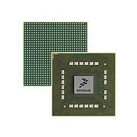
MPC8544VTALF Freescale Semiconductor, MPC8544VTALF Datasheet - Page 367

MPC8544VTALF
Manufacturer Part Number
MPC8544VTALF
Description
MPU POWERQUICC III 783-PBGA
Manufacturer
Freescale Semiconductor
Datasheets
1.MPC8544VTALF.pdf
(117 pages)
2.MPC8544VTALF.pdf
(2 pages)
3.MPC8544VTALF.pdf
(1340 pages)
Specifications of MPC8544VTALF
Processor Type
MPC85xx PowerQUICC III 32-Bit
Speed
667MHz
Voltage
1V
Mounting Type
Surface Mount
Package / Case
783-FCPBGA
Processor Series
MPC85xx
Core
e500
Data Bus Width
32 bit
Maximum Clock Frequency
667 MHz
Maximum Operating Temperature
+ 105 C
Mounting Style
SMD/SMT
Data Ram Size
32 KB
I/o Voltage
1.8 V, 3.3 V
Interface Type
I2C, HSSI, DUART
Minimum Operating Temperature
0 C
Lead Free Status / RoHS Status
Lead free / RoHS Compliant
Features
-
Lead Free Status / Rohs Status
Lead free / RoHS Compliant
Available stocks
Company
Part Number
Manufacturer
Quantity
Price
Company:
Part Number:
MPC8544VTALF
Manufacturer:
Freescale Semiconductor
Quantity:
10 000
Company:
Part Number:
MPC8544VTALFA
Manufacturer:
Freescale Semiconductor
Quantity:
10 000
- Current page: 367 of 1340
- Download datasheet (12Mb)
The address and command interface is also source synchronous, although 1/8 cycle adjustments are
provided for adjusting the clock alignment.
Figure 9-34
Figure 9-35
Figure 9-36
nine 8M × 8 DDR modules for a total of 256 Mbytes of system memory. One of the nine modules is used
for the memory’s ECC checking function. Certain address and control lines may require buffering.
Analysis of the device’s AC timing specifications, desired memory operating frequency, capacitive loads,
and board routing loads can assist the system designer in deciding signal buffering requirements. The DDR
memory controller drives 16 address pins, but in this example the DDR SDRAM devices use only 12 bits.
Freescale Semiconductor
shows an example DDR SDRAM configuration with four logical banks.
shows some typical signal connections.
shows an example DDR SDRAM configuration with four physical banks each comprised of
MCS, MRAS, MCAS, MWE
MPC8544E PowerQUICC III Integrated Host Processor Family Reference Manual, Rev. 1
Figure 9-34. Typical Dual Data Rate SDRAM Internal Organization
BANK ADDR
CKE, MCK, MCK
COMMAND:
ADDR
MRAS
MCAS
‘SUB’
MWE
MCS
MCK
MCK
Figure 9-35. Typical DDR SDRAM Interface Signals
CKE
BA1,BA0
DM
ADDR
DQM
13
2
SDRAM
Control
A[12:0]
BA[1:0]
Write Enable
64M x 1 Byte
Command
Bus
CK
512 Mbit
Data-Out Registers
Logical
Bank 0
DQ[7:0]
DQS
Logical
Bank 1
Read Data Latch
MUX, MASK,
Data Bus
8
Logical
Bank 2
Data-In Registers
DATA
DATA
STROBE
Logical
Bank 3
DDR Memory Controller
9-43
Related parts for MPC8544VTALF
Image
Part Number
Description
Manufacturer
Datasheet
Request
R
Part Number:
Description:
Manufacturer:
Freescale Semiconductor, Inc
Datasheet:
Part Number:
Description:
Manufacturer:
Freescale Semiconductor, Inc
Datasheet:
Part Number:
Description:
Manufacturer:
Freescale Semiconductor, Inc
Datasheet:
Part Number:
Description:
Manufacturer:
Freescale Semiconductor, Inc
Datasheet:
Part Number:
Description:
Manufacturer:
Freescale Semiconductor, Inc
Datasheet:
Part Number:
Description:
Manufacturer:
Freescale Semiconductor, Inc
Datasheet:
Part Number:
Description:
Manufacturer:
Freescale Semiconductor, Inc
Datasheet:
Part Number:
Description:
Manufacturer:
Freescale Semiconductor, Inc
Datasheet:
Part Number:
Description:
Manufacturer:
Freescale Semiconductor, Inc
Datasheet:
Part Number:
Description:
Manufacturer:
Freescale Semiconductor, Inc
Datasheet:
Part Number:
Description:
Manufacturer:
Freescale Semiconductor, Inc
Datasheet:
Part Number:
Description:
Manufacturer:
Freescale Semiconductor, Inc
Datasheet:
Part Number:
Description:
Manufacturer:
Freescale Semiconductor, Inc
Datasheet:
Part Number:
Description:
Manufacturer:
Freescale Semiconductor, Inc
Datasheet:
Part Number:
Description:
Manufacturer:
Freescale Semiconductor, Inc
Datasheet:


