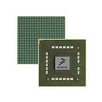
MPC8544VTALF Freescale Semiconductor, MPC8544VTALF Datasheet - Page 381

MPC8544VTALF
Manufacturer Part Number
MPC8544VTALF
Description
MPU POWERQUICC III 783-PBGA
Manufacturer
Freescale Semiconductor
Datasheets
1.MPC8544VTALF.pdf
(117 pages)
2.MPC8544VTALF.pdf
(2 pages)
3.MPC8544VTALF.pdf
(1340 pages)
Specifications of MPC8544VTALF
Processor Type
MPC85xx PowerQUICC III 32-Bit
Speed
667MHz
Voltage
1V
Mounting Type
Surface Mount
Package / Case
783-FCPBGA
Processor Series
MPC85xx
Core
e500
Data Bus Width
32 bit
Maximum Clock Frequency
667 MHz
Maximum Operating Temperature
+ 105 C
Mounting Style
SMD/SMT
Data Ram Size
32 KB
I/o Voltage
1.8 V, 3.3 V
Interface Type
I2C, HSSI, DUART
Minimum Operating Temperature
0 C
Lead Free Status / RoHS Status
Lead free / RoHS Compliant
Features
-
Lead Free Status / Rohs Status
Lead free / RoHS Compliant
Available stocks
Company
Part Number
Manufacturer
Quantity
Price
Company:
Part Number:
MPC8544VTALF
Manufacturer:
Freescale Semiconductor
Quantity:
10 000
Company:
Part Number:
MPC8544VTALFA
Manufacturer:
Freescale Semiconductor
Quantity:
10 000
- Current page: 381 of 1340
- Download datasheet (12Mb)
9.5.4.1
Freescale Semiconductor
•
•
•
•
If running with many devices, zero-delay PLL clock buffers, JEDEC-JESD82 standard, should be
used. These buffers were designed for DDR applications.
A 72 bit x 64 Mbytes DDR bank has 9-byte-wide DDR chips, resulting in 18 DDR chips in a
two-bank system. In this case, each MCK/MCK signal pair should drive exactly three devices.
PCB traces for DDR clock signals should be short, all on the same layer, and of equal length and
loading.
DDR SDRAM manufacturers provide detailed information on PCB layout and termination issues.
SDRAM Clock
Clock Distribution
MPC8544E PowerQUICC III Integrated Host Processor Family Reference Manual, Rev. 1
MDQ[0:63]
MDM[0:7]
MDQS
MCS0
MCS1
MRAS
MCAS
MWE
Figure 9-40. DDR SDRAM 4-Beat Burst Write Timing—ACTTORW = 4
MA n
ROW
0
1
ACTTORW
ROW
2
3
COL
4
D0
5
D1 D2 D3
COL
6
D0
7
D1 D2
COL
8
D3
00
D0
9
D1 D2 D3
COL
10
11
D0
DDR Memory Controller
D1 D2
12
D
9-57
Related parts for MPC8544VTALF
Image
Part Number
Description
Manufacturer
Datasheet
Request
R
Part Number:
Description:
Manufacturer:
Freescale Semiconductor, Inc
Datasheet:
Part Number:
Description:
Manufacturer:
Freescale Semiconductor, Inc
Datasheet:
Part Number:
Description:
Manufacturer:
Freescale Semiconductor, Inc
Datasheet:
Part Number:
Description:
Manufacturer:
Freescale Semiconductor, Inc
Datasheet:
Part Number:
Description:
Manufacturer:
Freescale Semiconductor, Inc
Datasheet:
Part Number:
Description:
Manufacturer:
Freescale Semiconductor, Inc
Datasheet:
Part Number:
Description:
Manufacturer:
Freescale Semiconductor, Inc
Datasheet:
Part Number:
Description:
Manufacturer:
Freescale Semiconductor, Inc
Datasheet:
Part Number:
Description:
Manufacturer:
Freescale Semiconductor, Inc
Datasheet:
Part Number:
Description:
Manufacturer:
Freescale Semiconductor, Inc
Datasheet:
Part Number:
Description:
Manufacturer:
Freescale Semiconductor, Inc
Datasheet:
Part Number:
Description:
Manufacturer:
Freescale Semiconductor, Inc
Datasheet:
Part Number:
Description:
Manufacturer:
Freescale Semiconductor, Inc
Datasheet:
Part Number:
Description:
Manufacturer:
Freescale Semiconductor, Inc
Datasheet:
Part Number:
Description:
Manufacturer:
Freescale Semiconductor, Inc
Datasheet:


