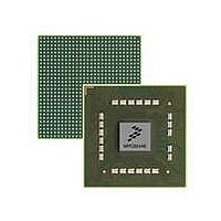
MPC8544VTALF Freescale Semiconductor, MPC8544VTALF Datasheet - Page 1328

MPC8544VTALF
Manufacturer Part Number
MPC8544VTALF
Description
MPU POWERQUICC III 783-PBGA
Manufacturer
Freescale Semiconductor
Datasheets
1.MPC8544VTALF.pdf
(117 pages)
2.MPC8544VTALF.pdf
(2 pages)
3.MPC8544VTALF.pdf
(1340 pages)
Specifications of MPC8544VTALF
Processor Type
MPC85xx PowerQUICC III 32-Bit
Speed
667MHz
Voltage
1V
Mounting Type
Surface Mount
Package / Case
783-FCPBGA
Processor Series
MPC85xx
Core
e500
Data Bus Width
32 bit
Maximum Clock Frequency
667 MHz
Maximum Operating Temperature
+ 105 C
Mounting Style
SMD/SMT
Data Ram Size
32 KB
I/o Voltage
1.8 V, 3.3 V
Interface Type
I2C, HSSI, DUART
Minimum Operating Temperature
0 C
Lead Free Status / RoHS Status
Lead free / RoHS Compliant
Features
-
Lead Free Status / Rohs Status
Lead free / RoHS Compliant
Available stocks
Company
Part Number
Manufacturer
Quantity
Price
Company:
Part Number:
MPC8544VTALF
Manufacturer:
Freescale Semiconductor
Quantity:
10 000
Company:
Part Number:
MPC8544VTALFA
Manufacturer:
Freescale Semiconductor
Quantity:
10 000
- Current page: 1328 of 1340
- Download datasheet (12Mb)
Memory space
Memory target queue
Message interrupts, see Interrupt controller (PIC), message
MMU assist registers (MAS0–MAS4, MAS6–MAS7),
MMUCFG (MMU configuration register), see e500 core,
MMUCSR0 (MMU control and status register 0), see e500
MODT[0:3] (DDR on-die termination) signals, 9-8
MRAS (DDR row address strobe) signal, 9-7
MSR (machine state register), see e500 core, registers
MSRCID[0:4] (DDR/LBC debug source ID) signals, 4-22,
MWE (DDR write enable) signal, 9-8
N
Nap mode, 1-20, 19-29
O
On-chip memory
Index-12
configuration, control, and status registers, 4-4
DDR controller, 9-9
debug, watchpoint, and trace buffer registers, 21-10
device memory map
DMA, 16-6
DUART, 13-4
ECM, 8-3
eTSEC, 15-13
global utilities, 19-3
I
interrupt controller (PIC), 10-9
L2 cache/SRAM, 7-8
LBC, 14-8
PCI/PCI-X, 17-11
performance monitor, 20-3
security engine (SEC), 12-10
PCI/PCI-X addressing, 17-47
performance monitor events, 20-18
see also Global utilities, power management
as L2 Cache, 1-13
as mapped SRAM, 1-13
overview, 1-12
2
C, 11-4
illegal interaction between local access windows and
address translation and mapping, 2-3
overview and example, 2-1
interrupts
6-35–6-39
registers
core, registers
14-8, 21-3, 21-7
DDR SDRAM chip selects, 2-9
MPC8544E PowerQUICC III Integrated Host Processor Family Reference Manual, Rev. 1
P
Page hit checking (LBC SDRAM), 14-50
Page management (LBC SDRAM), 14-50
PCI Express Base Specification, Rev. 1.0a
PCI Express controller
see PCI Express controller
accessing configuration space
address translation and mapping unit (ATMU)
block diagram, 18-2
clocks
commands
configuration space accesses, 18-42
error handling registers, 18-29–18-42
features, 18-3
latency timer, 18-49
modes of operation, 18-4
overview, 18-1
POR configuration, 18-4
power management, 18-13–18-18, 18-68–18-69
register descriptions
endpoint (EP) mode, 18-43
root complex (RC) mode, 18-42
inbound windows, 18-24
outbound windows, 18-19
minimum CCB frequency equation, 4-24
command register, 18-44
link width, 18-4
root complex or endpoint mode, 18-4
configuration header registers, 18-43–18-66
endpoint (EP) mode, 18-24
root complex (RC) mode, 18-25
32-bit memory base address register, 18-51
64-bit high memory base address register, 18-52
64-bit low memory base address register, 18-52
base address registers, 18-50–18-52, 18-57
bridge control register, 18-66
bus status register, 18-46
cache line size register, 18-48
capabilities pointer register, 18-54, 18-64
command register, 18-44
configuration and status register base address
device ID register, 18-44, 18-53
I/O base register, 18-59
I/O base upper 16 bits register, 18-63
I/O limit register, 18-59
I/O limit upper 16 bits register, 18-64
interrupt line register, 18-54, 18-65
interrupt pin register, 18-55, 18-65
latency timer register, 18-49, 18-59
maximum latency (EP-mode) register, 18-56
memory base register, 18-61
(PCSRBAR), 18-50, 18-57
Freescale Semiconductor
Related parts for MPC8544VTALF
Image
Part Number
Description
Manufacturer
Datasheet
Request
R
Part Number:
Description:
Manufacturer:
Freescale Semiconductor, Inc
Datasheet:
Part Number:
Description:
Manufacturer:
Freescale Semiconductor, Inc
Datasheet:
Part Number:
Description:
Manufacturer:
Freescale Semiconductor, Inc
Datasheet:
Part Number:
Description:
Manufacturer:
Freescale Semiconductor, Inc
Datasheet:
Part Number:
Description:
Manufacturer:
Freescale Semiconductor, Inc
Datasheet:
Part Number:
Description:
Manufacturer:
Freescale Semiconductor, Inc
Datasheet:
Part Number:
Description:
Manufacturer:
Freescale Semiconductor, Inc
Datasheet:
Part Number:
Description:
Manufacturer:
Freescale Semiconductor, Inc
Datasheet:
Part Number:
Description:
Manufacturer:
Freescale Semiconductor, Inc
Datasheet:
Part Number:
Description:
Manufacturer:
Freescale Semiconductor, Inc
Datasheet:
Part Number:
Description:
Manufacturer:
Freescale Semiconductor, Inc
Datasheet:
Part Number:
Description:
Manufacturer:
Freescale Semiconductor, Inc
Datasheet:
Part Number:
Description:
Manufacturer:
Freescale Semiconductor, Inc
Datasheet:
Part Number:
Description:
Manufacturer:
Freescale Semiconductor, Inc
Datasheet:
Part Number:
Description:
Manufacturer:
Freescale Semiconductor, Inc
Datasheet:


