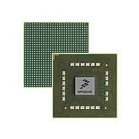
MPC8544VTALF Freescale Semiconductor, MPC8544VTALF Datasheet - Page 1309

MPC8544VTALF
Manufacturer Part Number
MPC8544VTALF
Description
MPU POWERQUICC III 783-PBGA
Manufacturer
Freescale Semiconductor
Datasheets
1.MPC8544VTALF.pdf
(117 pages)
2.MPC8544VTALF.pdf
(2 pages)
3.MPC8544VTALF.pdf
(1340 pages)
Specifications of MPC8544VTALF
Processor Type
MPC85xx PowerQUICC III 32-Bit
Speed
667MHz
Voltage
1V
Mounting Type
Surface Mount
Package / Case
783-FCPBGA
Processor Series
MPC85xx
Core
e500
Data Bus Width
32 bit
Maximum Clock Frequency
667 MHz
Maximum Operating Temperature
+ 105 C
Mounting Style
SMD/SMT
Data Ram Size
32 KB
I/o Voltage
1.8 V, 3.3 V
Interface Type
I2C, HSSI, DUART
Minimum Operating Temperature
0 C
Lead Free Status / RoHS Status
Lead free / RoHS Compliant
Features
-
Lead Free Status / Rohs Status
Lead free / RoHS Compliant
Available stocks
Company
Part Number
Manufacturer
Quantity
Price
Company:
Part Number:
MPC8544VTALF
Manufacturer:
Freescale Semiconductor
Quantity:
10 000
Company:
Part Number:
MPC8544VTALFA
Manufacturer:
Freescale Semiconductor
Quantity:
10 000
- Current page: 1309 of 1340
- Download datasheet (12Mb)
D
E
F
G
H
I
Freescale Semiconductor
MPC8544E PowerQUICC III Integrated Host Processor Family Reference Manual, Rev. 1
Direct-mapped cache. A cache in which each main memory address can appear in only
Double data rate. Memory that allows data transfers at the start and end of a clock cycle.
Effective address (EA). The 32-bit address specified for a load, store, or an instruction
Exclusive state. MEI state (E) in which only one caching device contains data that is also
Fetch. Retrieving instructions from either the cache or main memory and placing them
Flush. An operation that causes a cache block to be invalidated and the data, if modified,
Frame-check sequence (FCS). Specifies the standard 32-bit cyclic redundancy check
General-purpose register (GPR). Any of the 32 registers in the general-purpose register
Guarded. The guarded attribute pertains to out-of-order execution. When a page is
Harvard architecture. An architectural model featuring separate caches and other
Illegal instructions. A class of instructions that are not implemented for a particular
one location within the cache; operates more quickly when the memory request is
a cache hit.
thereby doubling the data rate.
fetch. This address is then submitted to the MMU for translation to either a
physical memory
in system memory.
into the instruction queue.
to be written to memory.
(CRC) obtained using the standard CCITT-CRC polynomial on all fields except
the preamble, SFD, and CRC.
file. These registers provide the source operands and destination results for all
integer data manipulation instructions. Integer load instructions move data from
memory to GPRs and store instructions move data from GPRs to memory.
designated as guarded, instructions and data cannot be accessed out-of-order.
memory management resources for instructions and data.
processor. These include instructions not defined by the architecture. In addition,
for 32-bit implementations, instructions that are defined only for 64-bit
implementations are considered to be illegal instructions. For 64-bit
implementations instructions that are defined only for 32-bit implementations are
considered to be illegal instructions.
address or an I/O address.
Glossary-3
Glossary
Related parts for MPC8544VTALF
Image
Part Number
Description
Manufacturer
Datasheet
Request
R
Part Number:
Description:
Manufacturer:
Freescale Semiconductor, Inc
Datasheet:
Part Number:
Description:
Manufacturer:
Freescale Semiconductor, Inc
Datasheet:
Part Number:
Description:
Manufacturer:
Freescale Semiconductor, Inc
Datasheet:
Part Number:
Description:
Manufacturer:
Freescale Semiconductor, Inc
Datasheet:
Part Number:
Description:
Manufacturer:
Freescale Semiconductor, Inc
Datasheet:
Part Number:
Description:
Manufacturer:
Freescale Semiconductor, Inc
Datasheet:
Part Number:
Description:
Manufacturer:
Freescale Semiconductor, Inc
Datasheet:
Part Number:
Description:
Manufacturer:
Freescale Semiconductor, Inc
Datasheet:
Part Number:
Description:
Manufacturer:
Freescale Semiconductor, Inc
Datasheet:
Part Number:
Description:
Manufacturer:
Freescale Semiconductor, Inc
Datasheet:
Part Number:
Description:
Manufacturer:
Freescale Semiconductor, Inc
Datasheet:
Part Number:
Description:
Manufacturer:
Freescale Semiconductor, Inc
Datasheet:
Part Number:
Description:
Manufacturer:
Freescale Semiconductor, Inc
Datasheet:
Part Number:
Description:
Manufacturer:
Freescale Semiconductor, Inc
Datasheet:
Part Number:
Description:
Manufacturer:
Freescale Semiconductor, Inc
Datasheet:


