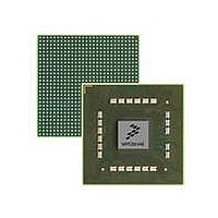
MPC8544VTALF Freescale Semiconductor, MPC8544VTALF Datasheet - Page 625

MPC8544VTALF
Manufacturer Part Number
MPC8544VTALF
Description
MPU POWERQUICC III 783-PBGA
Manufacturer
Freescale Semiconductor
Datasheets
1.MPC8544VTALF.pdf
(117 pages)
2.MPC8544VTALF.pdf
(2 pages)
3.MPC8544VTALF.pdf
(1340 pages)
Specifications of MPC8544VTALF
Processor Type
MPC85xx PowerQUICC III 32-Bit
Speed
667MHz
Voltage
1V
Mounting Type
Surface Mount
Package / Case
783-FCPBGA
Processor Series
MPC85xx
Core
e500
Data Bus Width
32 bit
Maximum Clock Frequency
667 MHz
Maximum Operating Temperature
+ 105 C
Mounting Style
SMD/SMT
Data Ram Size
32 KB
I/o Voltage
1.8 V, 3.3 V
Interface Type
I2C, HSSI, DUART
Minimum Operating Temperature
0 C
Lead Free Status / RoHS Status
Lead free / RoHS Compliant
Features
-
Lead Free Status / Rohs Status
Lead free / RoHS Compliant
Available stocks
Company
Part Number
Manufacturer
Quantity
Price
Company:
Part Number:
MPC8544VTALF
Manufacturer:
Freescale Semiconductor
Quantity:
10 000
Company:
Part Number:
MPC8544VTALFA
Manufacturer:
Freescale Semiconductor
Quantity:
10 000
- Current page: 625 of 1340
- Download datasheet (12Mb)
Table 14-2
Freescale Semiconductor
LCS[0:7]
Signal
LALE
LSYNC_OUT
LSYNC_IN
LUPWAIT/
LAD[0:31]
LCLK[0:2]
LSDRAS/
LSDCAS/
LA[27:31]
MSRCID
LGPL4/
contains detailed external signal descriptions for the LBC.
MDVAL
LGPL2
LGPL3
LPBSE
LGPL5
LBCTL
Name
LGTA/
LCKE
LOE/
LDP
I/O
MPC8544E PowerQUICC III Integrated Host Processor Family Reference Manual, Rev. 1
O External address latch enable. The local bus memory controller provides control for an external address
O Chip selects. Eight chip selects are provided which are mutually exclusive.
latch, which allows address and data to be multiplexed on the device signals.
Meaning
Meaning
State
State
Table 14-2. Local Bus Controller Detailed Signal Descriptions
Number of
Signals
Asserted/Negated—LALE is asserted with the address at the beginning of each memory
Asserted/Negated—Used to enable specific memory devices or peripherals connected to the
Table 14-1. Signal Properties—Summary (continued)
32
1
1
1
1
1
5
4
1
3
1
1
1
5
controller transaction. The number of cycles for which it is asserted is governed by the
ORn[EAD] and LCRR[EADC] fields. The exact timing of the negation of LALE is controlled
by the LBCR[AHD] field. Note that no other control signals are asserted during the
assertion of LALE.
LBC. LCS[0:7] are provided on a per-bank basis with LCS0 corresponding to the chip
select for memory bank 0, which has the memory type and attributes defined by BR0 and
OR0.
Input/Output Multiplexed address/data bus
Input/Output Local bus data parity
Direction
Output
Output
Output
Output
Output
Output
Output
Output
Output
Output
Output
Output
Output
Output
Output
Input
Input
Input
GPCM mode: output enable
SDRAM mode: row address strobe
UPM mode: general-purpose line 2
SDRAM mode: column address strobe
UPM mode: general-purpose line 3
GPCM mode: transaction termination
UPM mode: general-purpose line 4
UPM mode: external device wait
Local bus parity byte select
UPM mode: general-purpose line 5
Data buffer control
Local bus non-multiplexed address lsbs
Local bus clock enable
Local bus clocks
PLL synchronize input
PLL synchronize output
In LBC debug mode: local bus data valid
In LBC debug mode: local bus source ID
Description
Function
Local Bus Controller
14-5
Related parts for MPC8544VTALF
Image
Part Number
Description
Manufacturer
Datasheet
Request
R
Part Number:
Description:
Manufacturer:
Freescale Semiconductor, Inc
Datasheet:
Part Number:
Description:
Manufacturer:
Freescale Semiconductor, Inc
Datasheet:
Part Number:
Description:
Manufacturer:
Freescale Semiconductor, Inc
Datasheet:
Part Number:
Description:
Manufacturer:
Freescale Semiconductor, Inc
Datasheet:
Part Number:
Description:
Manufacturer:
Freescale Semiconductor, Inc
Datasheet:
Part Number:
Description:
Manufacturer:
Freescale Semiconductor, Inc
Datasheet:
Part Number:
Description:
Manufacturer:
Freescale Semiconductor, Inc
Datasheet:
Part Number:
Description:
Manufacturer:
Freescale Semiconductor, Inc
Datasheet:
Part Number:
Description:
Manufacturer:
Freescale Semiconductor, Inc
Datasheet:
Part Number:
Description:
Manufacturer:
Freescale Semiconductor, Inc
Datasheet:
Part Number:
Description:
Manufacturer:
Freescale Semiconductor, Inc
Datasheet:
Part Number:
Description:
Manufacturer:
Freescale Semiconductor, Inc
Datasheet:
Part Number:
Description:
Manufacturer:
Freescale Semiconductor, Inc
Datasheet:
Part Number:
Description:
Manufacturer:
Freescale Semiconductor, Inc
Datasheet:
Part Number:
Description:
Manufacturer:
Freescale Semiconductor, Inc
Datasheet:


