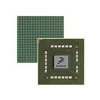
MPC8544VTALF Freescale Semiconductor, MPC8544VTALF Datasheet - Page 1101

MPC8544VTALF
Manufacturer Part Number
MPC8544VTALF
Description
MPU POWERQUICC III 783-PBGA
Manufacturer
Freescale Semiconductor
Datasheets
1.MPC8544VTALF.pdf
(117 pages)
2.MPC8544VTALF.pdf
(2 pages)
3.MPC8544VTALF.pdf
(1340 pages)
Specifications of MPC8544VTALF
Processor Type
MPC85xx PowerQUICC III 32-Bit
Speed
667MHz
Voltage
1V
Mounting Type
Surface Mount
Package / Case
783-FCPBGA
Processor Series
MPC85xx
Core
e500
Data Bus Width
32 bit
Maximum Clock Frequency
667 MHz
Maximum Operating Temperature
+ 105 C
Mounting Style
SMD/SMT
Data Ram Size
32 KB
I/o Voltage
1.8 V, 3.3 V
Interface Type
I2C, HSSI, DUART
Minimum Operating Temperature
0 C
Lead Free Status / RoHS Status
Lead free / RoHS Compliant
Features
-
Lead Free Status / Rohs Status
Lead free / RoHS Compliant
Available stocks
Company
Part Number
Manufacturer
Quantity
Price
Company:
Part Number:
MPC8544VTALF
Manufacturer:
Freescale Semiconductor
Quantity:
10 000
Company:
Part Number:
MPC8544VTALFA
Manufacturer:
Freescale Semiconductor
Quantity:
10 000
- Current page: 1101 of 1340
- Download datasheet (12Mb)
1
10–9
18.3.8.1.5
The revision ID register, shown in
.
18.3.8.1.6
The class code register, shown in
0x0B), sub-class (offset 0x0A), and programming interface (offset 0x09)—that indicate the basic
functionality of the function.
Freescale Semiconductor
Table 18-39
Bits
7–5
2–0
8
4
3
The error control and status bits in the command and status registers control PCI-compatible error reporting. PCI Express
advanced error reporting is controlled by the PCI Express device control register described in
Device Control
18.3.10.12.
Offset 0x08
Reset
W
Master data parity
R
Capabilities List All PCI Express devices are required to implement the PCI Express capability structure.
Interrupt Status
error detected
Name
Bits
7–0
—
—
—
7
describes the revision ID register fields.
MPC8544E PowerQUICC III Integrated Host Processor Family Reference Manual, Rev. 1
Register—0x54,” and the advance error reporting capability structure described in sections 18.3.10.1 through
PCI Express Revision ID Register—Offset 0x08
PCI Express Class Code Register—Offset 0x09
Table 18-38. PCI Express Status Register Field Descriptions (continued)
1
Table 18-39. PCI Express Revision ID Register Field Descriptions
Reserved
Set by the requestor (primary side for Type1 headers) when either the requestor receives a completion
marked poisoned or the requestor poisons a write request. Note that the parity error enable bit (bit 6)
in the command register must be set for this bit to be set.
Reserved
Set when an INTx interrupt message is pending internally to the device.
Note that this bit is associated with INTx messages and not Message Signaled Interrupts.
Reserved
Revision ID
Name
Figure 18-41. PCI Express Revision ID Register
Figure
Figure
Revision specific.
18-42, is comprised of three single-byte fields—base class (offset
18-41, is used to identify the revision of the device.
Revision specific
Revision ID
Description
Description
Section 18.3.9.8, “PCI Express
PCI Express Interface Controller
Access: Read-only
0
18-47
Related parts for MPC8544VTALF
Image
Part Number
Description
Manufacturer
Datasheet
Request
R
Part Number:
Description:
Manufacturer:
Freescale Semiconductor, Inc
Datasheet:
Part Number:
Description:
Manufacturer:
Freescale Semiconductor, Inc
Datasheet:
Part Number:
Description:
Manufacturer:
Freescale Semiconductor, Inc
Datasheet:
Part Number:
Description:
Manufacturer:
Freescale Semiconductor, Inc
Datasheet:
Part Number:
Description:
Manufacturer:
Freescale Semiconductor, Inc
Datasheet:
Part Number:
Description:
Manufacturer:
Freescale Semiconductor, Inc
Datasheet:
Part Number:
Description:
Manufacturer:
Freescale Semiconductor, Inc
Datasheet:
Part Number:
Description:
Manufacturer:
Freescale Semiconductor, Inc
Datasheet:
Part Number:
Description:
Manufacturer:
Freescale Semiconductor, Inc
Datasheet:
Part Number:
Description:
Manufacturer:
Freescale Semiconductor, Inc
Datasheet:
Part Number:
Description:
Manufacturer:
Freescale Semiconductor, Inc
Datasheet:
Part Number:
Description:
Manufacturer:
Freescale Semiconductor, Inc
Datasheet:
Part Number:
Description:
Manufacturer:
Freescale Semiconductor, Inc
Datasheet:
Part Number:
Description:
Manufacturer:
Freescale Semiconductor, Inc
Datasheet:
Part Number:
Description:
Manufacturer:
Freescale Semiconductor, Inc
Datasheet:


