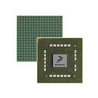
MPC8544VTALF Freescale Semiconductor, MPC8544VTALF Datasheet - Page 354

MPC8544VTALF
Manufacturer Part Number
MPC8544VTALF
Description
MPU POWERQUICC III 783-PBGA
Manufacturer
Freescale Semiconductor
Datasheets
1.MPC8544VTALF.pdf
(117 pages)
2.MPC8544VTALF.pdf
(2 pages)
3.MPC8544VTALF.pdf
(1340 pages)
Specifications of MPC8544VTALF
Processor Type
MPC85xx PowerQUICC III 32-Bit
Speed
667MHz
Voltage
1V
Mounting Type
Surface Mount
Package / Case
783-FCPBGA
Processor Series
MPC85xx
Core
e500
Data Bus Width
32 bit
Maximum Clock Frequency
667 MHz
Maximum Operating Temperature
+ 105 C
Mounting Style
SMD/SMT
Data Ram Size
32 KB
I/o Voltage
1.8 V, 3.3 V
Interface Type
I2C, HSSI, DUART
Minimum Operating Temperature
0 C
Lead Free Status / RoHS Status
Lead free / RoHS Compliant
Features
-
Lead Free Status / Rohs Status
Lead free / RoHS Compliant
Available stocks
Company
Part Number
Manufacturer
Quantity
Price
Company:
Part Number:
MPC8544VTALF
Manufacturer:
Freescale Semiconductor
Quantity:
10 000
Company:
Part Number:
MPC8544VTALFA
Manufacturer:
Freescale Semiconductor
Quantity:
10 000
- Current page: 354 of 1340
- Download datasheet (12Mb)
DDR Memory Controller
9.4.1.14
The DDR SDRAM clock control configuration register, shown in
adjustment.
Table 9-20
9.4.1.15
The DDR SDRAM initialization address register, shown in
used for the data strobe to data skew adjustment and automatic CAS to preamble calibration after POR.
9-30
Offset 0x130
Reset 0
9–31
Bits
0–4
5–8
W
R
0
CLK_ADJUST Clock adjust
0
describes the DDR_SDRAM_CLK_CNTL fields.
Name
—
—
—
0
DDR SDRAM Clock Control (DDR_SDRAM_CLK_CNTL)
DDR Initialization Address (DDR_INIT_ADDR)
MPC8544E PowerQUICC III Integrated Host Processor Family Reference Manual, Rev. 1
After the skew adjustment, this address will contain bad ECC data. This is
not important at POR, as all of memory should be subsequently initialized
if ECC is enabled (either by software or through the use of
DDR_SDRAM_CFG_2[D_INIT]).
If an HRESET has been issued after the DRAM is in self-refresh mode,
however, memory is not initialized, so this address should be written to
using an 8- or 32-byte transaction to avoid possible ECC errors if this
address could later be accessed.
0
0
4
Reserved
0000 Clock will be launched aligned with address/command
0001 Clock will be launched 1/8 applied cycle after address/command
0010 Clock will be launched 1/4 applied cycle after address/command
0011 Clock will be launched 3/8 applied cycle after address/command
0100 Clock will be launched 1/2 applied cycle after address/command
0101 Clock will be launched 5/8 applied cycle after address/command
0110 Clock will be launched 3/4 applied cycle after address/command
0111 Clock will be launched 7/8 applied cycle after address/command
1000 Clock will be launched 1 applied cycle after address/command
1001–1111 Reserved
Reserved
0
5
CLK_ADJUST
Table 9-20. DDR_SDRAM_CLK_CNTL Field Descriptions
Figure 9-15. DDR SDRAM Clock Control Configuration
1
0
Register (DDR_SDRAM_CLK_CNTL)
0
8
0
9
0 0 0 0 0 0 0 0 0 0 0 0 0 0 0 0 0 0 0 0 0
NOTE
Description
Figure
Figure
9-16, provides the address that will be
—
9-15, provides a 1/8-cycle clock
Freescale Semiconductor
Access: Read/Write
31
0
Related parts for MPC8544VTALF
Image
Part Number
Description
Manufacturer
Datasheet
Request
R
Part Number:
Description:
Manufacturer:
Freescale Semiconductor, Inc
Datasheet:
Part Number:
Description:
Manufacturer:
Freescale Semiconductor, Inc
Datasheet:
Part Number:
Description:
Manufacturer:
Freescale Semiconductor, Inc
Datasheet:
Part Number:
Description:
Manufacturer:
Freescale Semiconductor, Inc
Datasheet:
Part Number:
Description:
Manufacturer:
Freescale Semiconductor, Inc
Datasheet:
Part Number:
Description:
Manufacturer:
Freescale Semiconductor, Inc
Datasheet:
Part Number:
Description:
Manufacturer:
Freescale Semiconductor, Inc
Datasheet:
Part Number:
Description:
Manufacturer:
Freescale Semiconductor, Inc
Datasheet:
Part Number:
Description:
Manufacturer:
Freescale Semiconductor, Inc
Datasheet:
Part Number:
Description:
Manufacturer:
Freescale Semiconductor, Inc
Datasheet:
Part Number:
Description:
Manufacturer:
Freescale Semiconductor, Inc
Datasheet:
Part Number:
Description:
Manufacturer:
Freescale Semiconductor, Inc
Datasheet:
Part Number:
Description:
Manufacturer:
Freescale Semiconductor, Inc
Datasheet:
Part Number:
Description:
Manufacturer:
Freescale Semiconductor, Inc
Datasheet:
Part Number:
Description:
Manufacturer:
Freescale Semiconductor, Inc
Datasheet:


