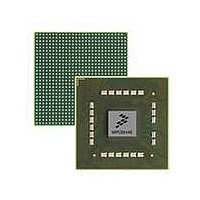
MPC8544VTALF Freescale Semiconductor, MPC8544VTALF Datasheet - Page 685

MPC8544VTALF
Manufacturer Part Number
MPC8544VTALF
Description
MPU POWERQUICC III 783-PBGA
Manufacturer
Freescale Semiconductor
Datasheets
1.MPC8544VTALF.pdf
(117 pages)
2.MPC8544VTALF.pdf
(2 pages)
3.MPC8544VTALF.pdf
(1340 pages)
Specifications of MPC8544VTALF
Processor Type
MPC85xx PowerQUICC III 32-Bit
Speed
667MHz
Voltage
1V
Mounting Type
Surface Mount
Package / Case
783-FCPBGA
Processor Series
MPC85xx
Core
e500
Data Bus Width
32 bit
Maximum Clock Frequency
667 MHz
Maximum Operating Temperature
+ 105 C
Mounting Style
SMD/SMT
Data Ram Size
32 KB
I/o Voltage
1.8 V, 3.3 V
Interface Type
I2C, HSSI, DUART
Minimum Operating Temperature
0 C
Lead Free Status / RoHS Status
Lead free / RoHS Compliant
Features
-
Lead Free Status / Rohs Status
Lead free / RoHS Compliant
Available stocks
Company
Part Number
Manufacturer
Quantity
Price
Company:
Part Number:
MPC8544VTALF
Manufacturer:
Freescale Semiconductor
Quantity:
10 000
Company:
Part Number:
MPC8544VTALFA
Manufacturer:
Freescale Semiconductor
Quantity:
10 000
- Current page: 685 of 1340
- Download datasheet (12Mb)
14.4.4.4.1
The RAM word is a 32-bit microinstruction stored in one of 64 locations in the RAM array. It specifies
timing for external signals controlled by the UPM.
and BSTn bits determine the state of UPM signals LCSn and LBS[0:3] at each quarter phase of the bus
clock.
Table 14-28
Freescale Semiconductor
10–11
Bits
8–9
12
0
1
2
3
4
5
6
7
Reset
Reset
W
W
R
R
CST1 CST2
G3T1 G3T3
16
0
Name
CST1
CST2
CST3
CST4
BST1
BST2
BST3
BST4
G1T1
G0H
G0L
describes RAM word fields.
MPC8544E PowerQUICC III Integrated Host Processor Family Reference Manual, Rev. 1
17
RAM Words
1
G4T1/DLT
Chip select timing 1. Defines the state (0 or 1) of LCS n during bus clock quarter phase 1.
Chip select timing 2. Defines the state (0 or 1) of LCS n during bus clock quarter phase 2.
Chip select timing 3. Defines the state (0 or 1) of LCS n during bus clock quarter phase 3.
Chip select timing 4. Defines the state (0 or 1) of LCS n during bus clock quarter phase 4.
Byte select timing 1. Defines the state (0 or 1) of LBS during bus clock quarter phase 1.
Byte select timing 2:. Defines the state (0 or 1) of LBS during bus clock quarter phase 2.
Byte select timing 3. Defines the state (0 or 1) of LBS during bus clock quarter phase 3.
Byte select timing 4. Defines the state (0 or 1) of LBS during bus clock quarter phase 4.
General-purpose line 0 lower. Defines the state of LGPL0 during the bus clock quarter phases 1 and
2 (first half phase).
00 Value defined by M x MR[G0CL]
01 Reserved
10 0
11 1
General-purpose line 0 higher. Defines the state of LGPL0 during the bus clock quarter phases 3 and
4 (second half phase).
00 Value defined by M x MR[G0CL]
01 Reserved
10 0
11 1
General-purpose line 1 timing 1. Defines the state (0 or 1) of LGPL1 during bus clock quarter phases
1 and 2 (first half phase).
CST3
18
3
2
G4T3/WAEN G5T1 G5T3
Figure 14-58. RAM Word Field Descriptions
Table 14-28. RAM Word Field Descriptions
CST4
19
3
BST1 BST2 BST3 BST4
20
4
21
5
Figure 14-58
All zeros
All zeros
22
6
REDO
Description
23
7
shows the RAM word fields. The CSTn
LOOP EXEN AMX
24
8
G0L
25
9
10 11
26 27
G0H G1T1 G1T3 G2T1 G2T3
NA
12
28
Access: Read/Write
Local Bus Controller
UTA TODT LAST
13
29
14
30
14-65
15
31
Related parts for MPC8544VTALF
Image
Part Number
Description
Manufacturer
Datasheet
Request
R
Part Number:
Description:
Manufacturer:
Freescale Semiconductor, Inc
Datasheet:
Part Number:
Description:
Manufacturer:
Freescale Semiconductor, Inc
Datasheet:
Part Number:
Description:
Manufacturer:
Freescale Semiconductor, Inc
Datasheet:
Part Number:
Description:
Manufacturer:
Freescale Semiconductor, Inc
Datasheet:
Part Number:
Description:
Manufacturer:
Freescale Semiconductor, Inc
Datasheet:
Part Number:
Description:
Manufacturer:
Freescale Semiconductor, Inc
Datasheet:
Part Number:
Description:
Manufacturer:
Freescale Semiconductor, Inc
Datasheet:
Part Number:
Description:
Manufacturer:
Freescale Semiconductor, Inc
Datasheet:
Part Number:
Description:
Manufacturer:
Freescale Semiconductor, Inc
Datasheet:
Part Number:
Description:
Manufacturer:
Freescale Semiconductor, Inc
Datasheet:
Part Number:
Description:
Manufacturer:
Freescale Semiconductor, Inc
Datasheet:
Part Number:
Description:
Manufacturer:
Freescale Semiconductor, Inc
Datasheet:
Part Number:
Description:
Manufacturer:
Freescale Semiconductor, Inc
Datasheet:
Part Number:
Description:
Manufacturer:
Freescale Semiconductor, Inc
Datasheet:
Part Number:
Description:
Manufacturer:
Freescale Semiconductor, Inc
Datasheet:


