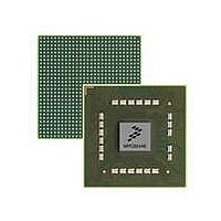
MPC8544VTALF Freescale Semiconductor, MPC8544VTALF Datasheet - Page 671

MPC8544VTALF
Manufacturer Part Number
MPC8544VTALF
Description
MPU POWERQUICC III 783-PBGA
Manufacturer
Freescale Semiconductor
Datasheets
1.MPC8544VTALF.pdf
(117 pages)
2.MPC8544VTALF.pdf
(2 pages)
3.MPC8544VTALF.pdf
(1340 pages)
Specifications of MPC8544VTALF
Processor Type
MPC85xx PowerQUICC III 32-Bit
Speed
667MHz
Voltage
1V
Mounting Type
Surface Mount
Package / Case
783-FCPBGA
Processor Series
MPC85xx
Core
e500
Data Bus Width
32 bit
Maximum Clock Frequency
667 MHz
Maximum Operating Temperature
+ 105 C
Mounting Style
SMD/SMT
Data Ram Size
32 KB
I/o Voltage
1.8 V, 3.3 V
Interface Type
I2C, HSSI, DUART
Minimum Operating Temperature
0 C
Lead Free Status / RoHS Status
Lead free / RoHS Compliant
Features
-
Lead Free Status / Rohs Status
Lead free / RoHS Compliant
Available stocks
Company
Part Number
Manufacturer
Quantity
Price
Company:
Part Number:
MPC8544VTALF
Manufacturer:
Freescale Semiconductor
Quantity:
10 000
Company:
Part Number:
MPC8544VTALFA
Manufacturer:
Freescale Semiconductor
Quantity:
10 000
- Current page: 671 of 1340
- Download datasheet (12Mb)
Note that during normal operation (read/write), a full 32-bit address that includes row and column is
generated on LAD[0:31]. However, address/data signal multiplexing implies that the address must be
latched by an external latch that is controlled by LALE. All SDRAM device address signals need to be
connected to the latched address bits and burst address bits (LA[27:31]) of the LBC, with the exception of
A10, which has a dedicated connection on LSDA10. LSDA10 is driven with the appropriate row address
bit for SDRAM commands that require A10 to be an address.
14.4.3.7
The software is responsible for setting correct values for device-specific parameters that can be extracted
from the device’s data sheet. The values are stored in the ORn and LSDMR registers. These parameters
include the following:
In addition, the LBC hardware ensures a default activate to precharge interval of 10 bus cycles. The
following sections describe SDRAM parameters programmed in LSDMR.
Freescale Semiconductor
•
•
•
•
•
•
Precharge to activate interval (LSDMR[PRETOACT])
Activate to read/write interval (LSDMR[ACTTORW])
CAS latency, column address to first data out (LSDMR[CL] and LCRR[ECL])
Write recovery, last data in to precharge (LSDMR[WRC])
Refresh recovery interval (LSDMR[RFRC])
External buffers on the control lines present (LSDMR[BUFCMD] and LCRR[BUFCMDC])
Activate Address (RAS):
R/W Address (CAS):
MPC8544E PowerQUICC III Integrated Host Processor Family Reference Manual, Rev. 1
SDRAM Device-Specific Parameters
Logical Address:
Figure 14-35. SDRAM Address Multiplexing
0
msbs
Row
Row
BS
BS
A n
BS
—
Row
Column
Column
To memory
device signals,
except A10
Local Bus Controller
lsbs
lsbs
lsbs
31
14-51
Related parts for MPC8544VTALF
Image
Part Number
Description
Manufacturer
Datasheet
Request
R
Part Number:
Description:
Manufacturer:
Freescale Semiconductor, Inc
Datasheet:
Part Number:
Description:
Manufacturer:
Freescale Semiconductor, Inc
Datasheet:
Part Number:
Description:
Manufacturer:
Freescale Semiconductor, Inc
Datasheet:
Part Number:
Description:
Manufacturer:
Freescale Semiconductor, Inc
Datasheet:
Part Number:
Description:
Manufacturer:
Freescale Semiconductor, Inc
Datasheet:
Part Number:
Description:
Manufacturer:
Freescale Semiconductor, Inc
Datasheet:
Part Number:
Description:
Manufacturer:
Freescale Semiconductor, Inc
Datasheet:
Part Number:
Description:
Manufacturer:
Freescale Semiconductor, Inc
Datasheet:
Part Number:
Description:
Manufacturer:
Freescale Semiconductor, Inc
Datasheet:
Part Number:
Description:
Manufacturer:
Freescale Semiconductor, Inc
Datasheet:
Part Number:
Description:
Manufacturer:
Freescale Semiconductor, Inc
Datasheet:
Part Number:
Description:
Manufacturer:
Freescale Semiconductor, Inc
Datasheet:
Part Number:
Description:
Manufacturer:
Freescale Semiconductor, Inc
Datasheet:
Part Number:
Description:
Manufacturer:
Freescale Semiconductor, Inc
Datasheet:
Part Number:
Description:
Manufacturer:
Freescale Semiconductor, Inc
Datasheet:


